Self-Retention of Data in Power-Gated Circuits Jun Seomun and Youngsoo Shin Department of Electrical Engineering, KAIST Daejeon 305-701, Korea
I. I NTRODUCTION Power gating [1], [2] is a circuit of choice to reduce subthreshold leakage current in CMOS circuits. It refers to cutting off a circuit from Vdd (by using a pMOS switch called a header) or from Vss (by using an nMOS switch called a footer) when it is not in use, i.e. during standby mode. The switch can be embedded in each logic gate, or it can be shared; the latter approach is de facto standard now in industry. When the switch is shared, a circuit is powered by Vdd and Vssv (when footer is used) or by Vddv and Vss (when header is used). The virtual power rails Vssv and Vddv are kept close to Vss and Vdd , respectively, in active mode; they are brought close to Vdd and Vss in standby mode, which is why leakage current in a circuit is cut off. This, however, implies that the circuit state, represented by primary outputs (POs) and flip-flops, are lost in standby. This may not be a problem in some systems, e.g. a DSP unit that can start from reset while it is supplied with a new data [3]. But, in many systems, at least a subset of data from POs and flip-flops has to be preserved for correct functionality after they are woken up or to provide correct data to circuits that are connected. This is made possible by employing an extra circuitry, in particular an isolator at PO and retention flipflop for storage. There are various implementations, which we review in Section II-A. These circuits inherently bring about the increase of area and wirelength, which should be clearly understood in quantitative manner, the topic of Section II-B; this can be used as a useful information during early stage of design. A new circuit, which we call self-data-retention, is proposed in Section III in an effort to remove wiring overhead caused by control signals of data retention circuits. A key idea is to monitor the potential change of virtual power rail to detect
978-1-4244-5035-0/09/$26.00 ©2009 IEEE
-212-
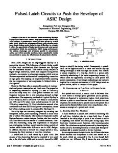
Vdd
1.2 1.164 V
1.0 N
Vssv
Voltage [V]
Abstract—Data retention is important to avoid data loss in power-gated circuits. Isolation circuitry should be used to keep output value as well as to avoid floating; a flip-flop capable of data retention, called retention flip-flop, should be used to keep flip-flop state. Examples of their implementations are reviewed. Due to extra circuitry and wires they introduce, it is important to understand how much increase of area and wirelength should be tolerated to support data retention, which we quantitatively analyze using several example circuits in 65-nm technology. A self-retention mechanism is proposed to alleviate the increase; it relies on the potential change of virtual power rail to detect the time for data retention and data restore thereby removing control signal implemented as extra wires and buffers in conventional power-gated circuits. Experiments show 8.6% decrease of wires on average.
Vssv
0.8 0.6 0.4
Vddv 0.2 0.073V
0 Power-gated block
Non-power-gated block
(a)
0
8 Time [�s]
16
(b)
Fig. 1. (a) Power-gated block interfaces with non-power-gated one, and (b) an example waveform of Vssv for s9234 in 1.2V 65nm technology after footer is turned off; a waveform of Vddv is also shown.
the time for data retention and for data restore. A new isolator and retention flip-flop that are specific to this circuit scheme, as well as several design considerations, are addressed. An experiment is conducted to validate the proposed circuit using example circuits in 65-nm technology, which shows 8.6% decrease of wires on average. II. DATA R ETENTION OF P OWER -G ATED C IRCUIT A. Data retention 1) Output Isolation: Fig. 1(a) shows a power-gated block that interfaces with the non-power-gated one. Once the footer is turned off, Vssv increases towards Vdd but very slowly as illustrated in Fig. 1(b); the node N corresponding to PO of the power-gated block is also charged. This causes two problems: a large amount of short-circuit current flows through the inverter due to very slow change of N ; the value of N is kept to high irrespective of its original value before the footer is turned off, implying that the inverter may receive a wrong value. The same logic applies when header is used; waveform of Vddv when it is turned off is also shown in Fig. 1(b). The circuit shown in Fig. 2(a) has to be inserted at N to alleviate these problems. The out is de-coupled from in once fence is asserted; the latch then delivers the output value, which it stores. The circuit, however, causes extra delay as well as area and power consumption. Their use should be limited whenever it is possible. Simple pMOS or nMOS can be used instead as shown in Fig. 2(b) when keeping the output from floating is the only objective, i.e. when the output value itself does not necessarily need to be preserved. When footer is used, a helper pMOS sets out to high; a helper nMOS is employed when header is used and sets out to low; the helper devices remain off in active mode. Isolator and hold circuit shown in
ISOCC 2009
TABLE I I NCREASE OF AREA AND WIRELENGTH OF POWER - GATED CIRCUITS
fence fence
fence fence
Name c5315 c6288 s5378 b21
fence out
in (a)
# Comb. 662 1232 680 16639
# FFs 0 0 176 490
# POs 123 32 49 22
Flip-flop Isolator Footer
80%
out in
ΔWirelength (%) 17 6 17 9
100%
100%
fence in
ΔArea (%) 46 13 41 3
out
Etc Connection to Vss Sleep
80%
60%
60%
40%
40%
20%
20%
fence (b)
Fig. 2.
(a) An example isolator and (b) hold circuits. 0%
0%
c RET
RET c
NL
CLK
GL
GL
RET
Fig. 3.
Fig. 4.
c GL
GL
c
RET
s5378
b21
c5315
c6288
s5378
b21
(b)
NL
GL
GL
c6288 (a)
c D
c5315 NL
GL
: Low-Vt
c
Normalized increase of (a) area and (b) wirelength.
Q
by using normal flip-flops if the remaining voltage drop within a circuit is large enough. This, however, comes at the cost of increased leakage in a circuit.
: High-Vt GL: Gated logic NL: Non-gated logic
B. Implication of Data Retention on Physical Design
An example of retention flip-flop.
Fig. 2 are usually used together in practical circuits; which PO should be associated with isolator is thus a design problem. 2) Storage Retention: To preserve the contents of storage elements, there are two approaches [3]: use a scan chain or substitute retention registers for normal ones. In the first approach, a whole circuit can be power-gated after data backup via scan-out, which is an advantage. Scan-in and scan-out may take long time and dissipate extra power, which are disadvantages. Thus, this approach is justified only when standby period is very long. There are varying implementations of retention registers [4]–[7]. Fig. 3 shows an example, where conventional master-slave D flip-flop is used with slight modification for data retention. The slave latch is directly connected to Vdd and Vss (thus denoted by NL) while the remainder is connected to current switches (denoted by GL). The internal signal c is forced to 0, which allows retention in slave latch, by using pull-down nMOS with RET set to 1 (set to 0 in active mode). Retention flip-flops invariably cause area increase of 30% ∼ 50% in addition to increase of sequencing overhead, increase of wires, and power consumption. Their use also should be limited. There are also circuits that do not require explicit control for data retention, i.e. data is implicitly retained. Dynamic retention flip-flop [8] eliminates sleep control signal by preserving the state in internal DRAM cells; the amount of retention, however, is very short. Virtual power/ground rails clamp (VRC) [9] uses forward biased diodes placed in parallel with current switches. When current switches are turned off, virtual power rails start to float but are clamped by the built-in potential of the diode; thus, retention is implicitly performed
-213-
Isolators and retention flip-flops introduce extra circuitry and wires. Therefore, it is important to understand how much increase of area and wirelength should be tolerated in supporting data retention and what exactly contribute to that increase, which could be used as a useful information during early stage of design, e.g. architectural design. Four example circuits summarized in Table I were taken for a quantitative analysis. The first two are purely combinational while the other two are sequential. After each circuit was synthesized in 65nm technology, data retention was assumed at all POs and flip-flops by using a circuit shown in Fig. 2(a) and Fig. 3, respectively. Footer was sized assuming voltage drop of 1% of Vdd across it during active mode. The last two columns of Table I show the increase of area and wirelength over the designs that do not use power gating. The area corresponds to the sum of the areas of all the cells. For routing, about 85% of placement region was forced to be occupied by the cells and metal layers up to M4 were allowed for automatic routing. Fig. 4 further analyzes each increase by showing the contribution from various components. There is fairly a large increase of area in c5315. This is because of its large number of POs (considering its combinational gates), thus of the same number of isolators that are introduced, which can be identified in Fig. 4(a). The c6288 has smaller number of POs, thus causes less increase of area, though the absolute increase is still sizable due to footers, which can be identified in Fig. 4(a). The increase due to footer alone is about 9% and 47% in these two circuits. In two sequential circuits, area increase is dominated by retention flipflops; each retention flip-flop we used is 52% bigger than its non-power-gated counterpart. By comparing s5378 and b21 in
ISOCC 2009
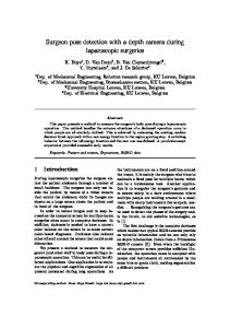
Vdd
G2 Sleep charge SP pump
Comb. logic
Retention flip-flop SLP
Pulse generator
Vssv
fence
NL
fence
Isolator
fence
SLP
NL
sleep
fence
SP
in
Vssv
N1
NL
: Low-Vt
Footer
sleep
NL
G1 out
NL
: High-Vt GL: Gated logic NL: Non-gated logic
(a)
Fig. 5.
Power-gated circuit with self-data-retention. c Vssv
Table I, it can be seen that area increase is largely determined by the proportion of flip-flops. There are three components in wirelength increase as shown in Fig. 4(b): extra wires for sleep signal, connection of data retention elements to Vdd or Vss rails, and the increase of all other signal wires due to increased wiring congestion. Table I should be considered as an extreme, since data retention was assumed at all POs and flip-flops. The increase in practical circuits would thus vary depending on the proportion of POs and flip-flops that are retained.
RET
NL
RET
NL
c NL
GL
c
c
D
GL
GL
CLK
GL
GL
GL
GL
Q
RET c
c
RET
(b)
Fig. 6.
(a) Isolator and (b) flip-flop with self-data-retention.
III. S ELF -DATA -R ETENTION A. Overview Fig. 5 illustrates the concept of self-data-retention. The isolators and retention flip-flops are not controlled by sleep control signal but by Vssv , which is a power rail. Therefore, each retention element can be connected to local Vssv rather than to external controller, thereby eliminating any wires and buffers between the element and controller. When the footer is turned off, Vssv rises towards Vdd but very slowly as we discussed in conjunction with Fig. 1. If we directly use Vssv , which takes too long to rise, for SLP inputs of isolators and retention flip-flops, the data cannot be properly captured and preserved, and large amount of shortcircuit current may flow during transition. This is alleviated by employing a large pMOS switch located between Vdd and Vssv , which we call sleep charge pump (SCP), as shown in Figure 5; the SCP is driven by a pulse generator. Once sleep goes high (sleep goes low) to make a transition to standby mode, the pulse generator produces a short pulse that briefly turns on the SCP, which in turn allows Vssv to rise towards Vdd in short amount of time. The size of SCP and the width of pulse applied to it are important design considerations that will be addressed in Section III-C. The SCP is implemented as more than one switches distributed over the layout and the same is applied to pulse generator. Their physical location, therefore, is important, which is also addressed in Section III-C. B. Design of Isolator and Flip-Flop Fig. 6(a) shows an isolator with self-data-retention, which is based on Fig. 2(a). When Vssv is low (active mode), fence is low that allows the circuit to be transparent, i.e. out = in. When in is high and the footer turns off (Vssv starts to rise towards Vdd ), it is readily seen that N1 can be safely captured
-214-
in the latch. When in is low and the footer turns off, however, care needs to be taken to guarantee the integrity of N1 , because in eventually becomes high in standby mode. In order to ensure that G1 becomes high-impedance well before rising in starts to impact N1 , nMOS device in G2 is not stacked (at the cost of increased subthreshold leakage) so that fence arrives early enough at G1 , and high-Vt is employed at G1 (at the cost of increased delay) so that in does not propagate to N1 too early. We implemented the isolator in 1.2 V, 65-nm CMOS technology and compared it to conventional isolator shown in Fig. 2(a). The area and delay increase by 25% and 30%, respectively, due to the stacked inverters. Leakage current (both active and standby) is reduced by 22% due to the use of high-Vt in G1 . A flip-flop with self-data-retention can be designed in a similar way as shown in Fig. 6(b). Its implementation shows the area increase by 8% but without any delay increase. Leakage current (both active and standby) remains almost the same. C. Design Considerations The size of SCP and pulse width are important, because they determine the amount of time Vssv takes to reach its steady state (thus the delay for making transition to standby mode) and the amount of energy dissipated during the period (thus transition energy). It can be readily shown that the best size and width are achieved by ensuring that the total amount of charge supplied by SCP is no less than the amount needed to charge Vssv to Vdd . This is done by equating the total amount of charge supplied by SCP and the total amount of charge that we need to charge Vssv up to Vdd . The former is a function of SCP size and pulse width; the latter is proportional to the capacitance involved in Vssv rails and load capacitances that
ISOCC 2009
60�m
Pulse generator Footers
SCPs
25�m
Vss
Fig. 7.
Placement of SCPs, pulse generators, and footers.
TABLE II R EDUCTION OF TOTAL WIRELENGTH AND AVERAGE CONGESTION Name s35932 s38417 s38584 b12 b13 aes1 irda1 irda2 irda3 i2c1 mc1 mc2 ram1 rng wb1 Average
# Gates
# FFs
# POs
3513 3333 4294 855 240 503 160 697 160 312 122 252 1984 118 604
1728 1564 1275 119 53 227 32 96 32 49 17 74 1024 112 274
320 106 304 6 10 129 33 4 1 8 32 68 8 32 362
Vssv (V) 1.15 1.14 1.15 1.16 1.13 1.15 1.19 1.14 1.19 1.17 1.14 1.17 1.16 1.20 1.12 1.16
Reduction (%) Wirelength Cong. 5.1 4 8.5 5 4.9 4 12.7 5 13.6 4 7.3 6 6.4 1 7.6 3 12.5 3 15.4 4 10.5 4 5.6 4 4.8 4 11.2 2 3.3 8 8.6 4
are electrically connected to Vssv through turned-on pull-down networks. Once the numbers of SCPs, pulse generators, and footers are determined, they are placed as illustrated in Fig. 7. The SCPs are placed in a regular fashion, with a distance of about 25 μm between adjacent SCPs; the channel width of each SCP cell is 7.2 μm. The pulse generator was designed to drive up to 4 SCPs with a slew constraint of 350 ps. The footers are also placed in a regular fashion. D. Experiments We carried out experiments on a set of sequential circuits taken from the ISCAS and ITC benchmarks. We also included circuits extracted from several open cores [10] including a cryptography core, communication controller, and memory controller. Columns 2–4 of Table II are the number of combinational gates, flip-flops, and POs. Each circuit was synthesized [11] with commercial 1.2 V, 65-nm bulk CMOS technology. The fifth column corresponds to the potential of Vssv set by SCP; it is charged up to 1.16 V on average (97%
-215-
of 1.2 V). To assess the effectiveness on wiring congestion and total wirelength, each netlist was placed and routed [12]. We forced about 85% of placement region to be occupied by the cells in each circuit, which is a tight placement; metal layers up to M3 were allowed for routing; the placement region was divided into a grid with individual square size of 1.6 μm × 1.6 μm for computing congestion. Self-data-retention has fewer wires (than conventional power gating) by 8.6% on average as shown in the sixth column. There are two factors that have a combined effect on the reduced wirelength: self-data-retention does not have wires for the control signal of retention flip-flops and isolators; this lack of wires helps automatic router reduce other signal wires. The last column reports the average congestion, which is reduced by 4% on average. The reduction on wirelength and congestion comes at the cost of increased area by 6.8% on average. IV. S UMMARY We have reviewed data retention of power-gated circuits, in particular isolator to avoid floating and to keep output value, and retention flip-flop to keep its state. The implication of these retention circuits on area and wirelength should be understood, which could be used as a useful information during early stage of design. The quantitative analysis has been performed by using example circuits in 65-nm technology. The concept of self-data-retention has been introduced in an effort to remove wiring overhead caused by control signals of data retention circuits. It has been experimentally shown that wires can be reduced by 8.6% on average. R EFERENCES [1] M. Horiguchi, T. Sakata, and K. Itoh, “Switched-source-impedance CMOS circuit for low standby subthreshold current giga-scale LSI’s,” IEEE Journal of Solid-State Circuits, vol. 28, no. 11, pp. 1131–1135, Nov. 1983. [2] S. Mutoh et al., “A 1-V power supply high-speed digital circuit technology with multithreshold-voltage CMOS,” IEEE Journal of SolidState Circuits, vol. 30, no. 8, pp. 847–854, Aug. 1995. [3] M. Keating et al., Low Power Methodology Manual For System-on-Chip Design. Springer, 2007. [4] S. Shigematsu et al., “A 1-V high-speed MTCMOS circuit scheme for power-down application circuits,” IEEE Journal of Solid-State Circuits, vol. 32, no. 6, pp. 861–869, June 1997. [5] V. Zyuban and S. V. Kosonocky, “Low power integrated scan-retention mechanism,” in Proc. Int. Symp. on Low Power Electronics and Design, Aug. 2002, pp. 98–102. [6] H.-S. Won et al., “An MTCMOS design methodology and its application to mobile computing,” in Proc. Int. Symp. on Low Power Electronics and Design, Aug. 2003, pp. 110–115. [7] H. Mair et al., “A 65-nm mobile multimedia applications processor with an adaptive power management scheme to compensate for variations,” in Proc. Symp. on VLSI Circuits, June 2007, pp. 224–225. [8] S. Henzler, G. Georgakos, M. Eireiner, T. Nirschl, C. Pacha, J. Berthold, and D. Schmitt-Landsiedel, “Dynamic state-retention flip-flop for finegrained power gating with small design and power overhead,” IEEE Journal of Solid-State Circuits, vol. 41, no. 7, pp. 1654–1661, 2006. [9] K. Kumagai, H. Iwaki, H. Yoshida, H. Suzuki, T. Yamada, and S. Kurosawa, “A novel powering-down scheme for low Vt cmos circuits,” in Proc. Symp. on VLSI Circuits, June 1998, pp. 44–45. [10] “Opencores,” http://www.opencores.org/. [11] Synopsys, “Design compiler user guide,” Mar. 2007. [12] ——, “Astro User Guide,” June 2006.
ISOCC 2009