Register Grouping for Synthesis of Clock Gating Logic Inhak Han‡ , Jonggyu Kim† , Joonhwan Yi† and Youngsoo Shin‡ of Electrical Engineering, KAIST, Daejeon 34141, Korea † Department of Computer Engineering, University of Kwangwoon, Seoul 01897, Korea ‡ School
Abstract—Clock gating logic is typically specified by designers in register transfer level (RTL). Its automatic synthesis is not only convenient but also complements RTL clock gating by extracting additional gating conditions. A key in automatic synthesis of clock gating logic is grouping registers that will share the same gating logic. A new grouping method based on iterative maximum weight matching is proposed. Clock gating implementation with the proposed method reduces power consumption by 40% on average with our test circuits.
I. I NTRODUCTION Clock gating has become a standard practice to reduce power consumption in synchronous circuit designs. It involves the conversion of a load-enable register shown in Fig. 1(a) into the standard register with clock gating cell (CGC) shown in Fig. 1(b). The condition when clock is gated, called gating logic or gating function, is typically specified by designers. A latch is included in CGC to remove potential glitches from gating function. If gating function is not specified, it may be automatically extracted from the input and output logic of registers. The first step is to identify each individual gating function fi of flipflop (FF) i. If input di and output qi take the same value, there is no need to load the input so fi can be set to 1 and clock is gated: (1) fi = di ⊕ qi , where ⊕ denotes XOR. Note that qi is a primary input and di is a function of primary inputs. A direct implementation of (1), also called XOR-self gating [1], involves an XOR gate and a CGC; this however can only be applied when di arrives sufficiently early so that a delay through the XOR gate and the CGC can be tolerated. Alternative approach is to implement fi as a separate logic. It is however impractical to introduce gating logic for each individual fi . We thus have to group fi s so that the corresponding FFs in the same group are driven by a single gating function: F = f1 ∧ f2 ∧ · · · ∧ fn ,
(2)
where ∧ denotes AND. The probability that F is evaluated to 1, denoted by P r(F ), is called gating probability and satisfies P r(F ) ≤ min P r(fi ). i
(3)
The problem is then to group FFs in such a way that those in the same group have similar gating functions, while
d Gating function
Gating function
q
d
CLK CGC
CLK (a)
Fig. 1.
(b)
(a) Load-enable register and (b) standard register with clock gating.
minimizing the number of groups (or CGCs) and maximizing the gating probability. It turns out that the grouping problem is a multi-objective problem. A. Related Work There have been two main studies of register grouping: one adopts the technique to group similar gene expression patterns, called CAST, in standard clock gating [2]; the other introduces grouping technique in XOR-self gating [3]. The former merges similar gating functions as the form of (2), while defining the similarity between fi and fj as the proportion of |fi ∧ fj | to |fi ∨ fj |, where |f | denotes the size of the on-set of f . It iteratively performs the following steps: the pair of fi and fj with maximum similarity is merged into F (i.e. F = fi ∧ fj ); and the fi , whose similarity to F is maximum, is repeatedly merged into F (i.e. F = fi ∧ F ), until no more fi , whose similarity to F is larger than a userdefined value, exists. It is useful only when every pair of fi and fj in different F ’s of the final solution has low similarity, which is the feature of gene expression patterns. The latter suggests a grouping method which maximizes average gating probability while applying clock gating to all the FFs whose timing slack is sufficient. XOR-self gating, however, can be applied to only small number of FFs due to rigid timing constraint. Thus, its power saving is essentially smaller compared to standard clock gating and we do not compare it with our method. B. Contributions In this paper, we propose a new register grouping method based on iterative maximum weight matching. Two additional grouping schemes, a simple greedy approach and the one using CAST algorithm [2], are also implemented to compare with our method. Experiments on test circuits show that clock gating with our method reduces power consumption between 13% and 55%, with an average of 40%; and 35% and 25%
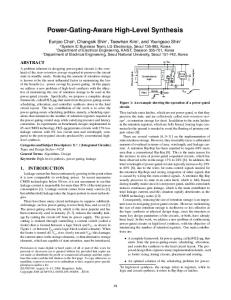
q
v2 1.2 0.8 0.1 0.1 v1 1.1 0.2 0.6 v3 1.3
0.4
1.6 v5 -0.3 v4 0.4 1.4 v7 1.8 0.3 0.3 0.5 1.4 v6 0.1
v’1 {v1,v2} -0.3
1.5
-0.2 0.5
v’2 3.0 {v4,v5}
v’1 {v1,v2,v3} 2.3
-0.4
v’2 {v4,v5}
v’1 {v1,v2,v3} 1.5
0.1
1.2 v5
3.0
v’1 {v1,v2,v3,v5}
v’2 {v4,v5}
2.6
2.3
-0.4 -0.1
-0.3 v3 1.3
0.1
2.3
v’3 {v6,v7}
(b)
(a)
-0.4 v’3 2.3 {v6,v7}
v4 v4 1.2
2.3
v’2 {v6,v7}
(d)
(c)
1.2 (e)
Fig. 2. An example of iterative MWM grouping process: (a) initial graph (not all edges are shown for simplicity of presentation), (b) after first and (c) second MWM, (d) after assessment of power saving, and (e) after additional iterative MWM; where each dashed edge has negative weight.
reductions were respectively observed with two approaches, a simple greedy and CAST. II. R EGISTER G ROUPING Given a gate-level netlist without clock gating, we first extract gating function fi and gating probability P r(fi ) of each FF i. The function fi is identified using (1) and the probability P r(fi ) is obtained using simulation-based approach1 [4]. The proposed approach is performed in three steps: grouping FFs, to minimize circuit’s power consumption, under the assumption that all FFs are applied clock gating; determining if each FF group (register) is applied clock gating or not by assessing power saving followed by disassembling each register that fails the assessment; and finding more groups with ungrouped FFs. The problem toward the first step can be stated as follows: given a set of FFs, each of which is applied clock gating with fi , the goal is to find a set of registers where the FFs in each register Rj is gated together by Fj = ∧i∈Rj fi , while minimizing the sum of the power dissipated by each Rj ’s and ungrouped FFs. A. Graph Formulation A graph G = (V, E, {P }, {P S}) is set up to solve the problem, as shown in Fig. 2(a), in which each vertex vi ∈ V corresponds to a FF i; and each edge (vi , vi� ) ∈ E indicates a potential group of the FFs corresponding to vi and vi� . Each vertex vi is associated with P (vi ), which is the power consumed by i when clock gating is applied with fi : PCGC + P (fi ) + PF F (1 − P r(fi )),
(4)
where PCGC , P (fi ), and PF F respectively denote power consumption of CGC, of fi , and of ungated FF. For each edge between vi and vi� , P S((vi , vi� )) is assigned, which is the amount of power saving if fi and fi� are merged into F = fi ∧ fi� : PCGC + (P (fi ) + P (fi� ) − P (F )) − 2PF F ΔP r(fi , fi� ), (5) where the first term is due to the reduction in CGCs (from two to one); the second corresponds to the saving from merged gating functions; and the last represents the increase 1 We implement f in a circuit imaginarily and apply N number of patterns i to the input of a circuit. P r(fi ) is then computed by dividing the number of 1’s in the list of the outputs of fi by N .
of power due to decreased gating probability after merge. The term ΔP r(fi , fi� ) denotes the average decrease of gating probability after merge, which is computed by (P r(fi ) + P r(fi� ))/2 − P r(F ). As grouping proceeds, FFs are combined in Rj and the corresponding vertices coalesce into one super vertex vj� associated with P (vj� ): PCGC + P (Fj ) + |vj� | · PF F (1 − P r(Fj )),
(6)
where |vj� | denotes the number of vertices in vj� . The problem can now be defined as to find a set of disjoint super vertices {vj� }, while minimizing the sum of all P (vj� ) and all P (vi ) where vi is not included in any super vertex vj� . B. Algorithm The set of disjoint super vertices, which minimizes the sum of vertex weights, can now be found using maximum weight matching (MWM), i.e. picking a set of edges such that any pair of edges does not share a common vertex, while the sum of edge weights is maximized. The grouping problem can be effectively solved via MWM. The proposed approach is explained using an example shown in Fig. 2. Given a graph G, the edges with negative weights are deleted like the dashed edge (v5 , v7 ) in Fig. 2(a); note that now all the edges in G have non-negative weights. The problem is now subject to MWM. Let the three thick edges in Fig. 2(a) be a solution. Each thick edge is then contracted, i.e. the edge is removed from G and its two incident vertices are merged into a super vertex. A new graph is set up as shown in Fig. 2(b), where v1� , v2� , and v3� are super vertices. Assuming that the edge between v1� and v3 is contracted this time leads us to Fig. 2(c). MWM repeats until all edges have negative weights. MWM can be solved in O(V 2 E) [5], where V and E represent the number of vertices and edges, respectively. The complexity of the proposed process is thus O(V 3 E) since one pair of vertices are merged at each iteration in the worst case. Each vertex is then checked to see whether applying clock gating is beneficial in terms of power consumption: PF F > P (vi ) or |vj� | · PF F > P (vj� ). Assume that the vertex v2� = {v4 , v5 } fails the assessment. v2� is then ungrouped and the weights of the vertices v4 and v5 are changed to PF F , as illustrated in Fig. 2(d).
Gating logic
Comb. gates
FFs
CGCs
Normalized power
1.0 0.8 0.6 0.4 0.2
Fig. 3.
wb_conmax
sasc
ps2
i2c
aes
b13
b12
b11
s38417
s35932
s15850
s13207
0.0
Power consumption of circuits after clock gating using CAST (left-hand bars), greedy (center bars), and iterative MWM (right-hand bars).
Since the vertices that fail the assessment of power saving are ungrouped and their weights are changed, MWM can find other groups that achieve power saving. We again iterate MWM until all edges have negative weights, which produces the graph shown in Fig. 2(e). C. Gating Logic Implementation Gating logic F has to be implemented during register grouping to compute P (F ). Direct implementation of F may involve too much extra logic [6]. Two techniques, namely approximation and simplification, have been introduced. 1) Approximation: The on-set of F can be considered as a don’t-care set, because a circuit operates correctly if clock is gated or not when gating is possible (F = 1). Thus, F can be approximated by any function F � whose on-set is a subset of the on-set of F ; the product terms associated with lower probability can form a don’t-care set and then the sum of the remaining terms constitutes F � [6]. 2) Simplification: F can be simplified into DQ + R using Boolean division [7], where D corresponds to some existing logic. It is thus only necessary to implement logic for quotient Q and remainder R. In this paper, every gating function F is approximated to F � by forming the product terms with probability less than 0.001 as a don’t care set and F � is synthesized using division, to obtain implementable logic in terms of runtime and the number of extra gates. Power consumption of gating logic is estimated as the average power consumption of the division form of F � and P r(F � ) is used as gating probability. III. E XPERIMENTAL R ESULTS A set of test circuits was compiled from ISCAS and ITC benchmarks, as well as from open cores [8]. The number of combinational gates and FFs in the initial netlist, which was obtained by logic synthesis [9] with a 28-nm ASIC gate library, are given in Table I. The algorithms of register grouping and gating logic synthesis were implemented in SIS [10].
The power consumption after applying clock gating with three grouping schemes, CAST, greedy, and proposed iterative MWM, is shown in Fig. 3. It is normalized to the power of original circuit (i.e. without clock gating). The power consumption of the circuits before and after clock gating was obtained by simulating each circuit with a fast transistorlevel simulator [11] and applying 1000 input patterns. CAST was implemented as explained in Section I-A with userdefined value of 0.7. Greedy was done by iteratively merging two vertices with maximum edge weight from G. In both approaches, assessment of power saving and ungrouping is performed lastly. There are three factors that determine the efficiency of register grouping in terms of power consumption: • Number of CGCs: CGC draws power (0.8μW) as much as ungated FF (1.2μW), so it is important to use as few as possible. • Average gating probability: The average gating probability clearly drops as we try to minimize the number of CGCs, so we have to group FFs while keeping gating probability as high as possible. • Extra logic to implement gating functions: As shown in Fig. 3, the power consumption of gating logic is marginal in most circuits except circuits b12 and ps2. This is expected due to smaller switching activity of gating logic compared to typical combinational logic. Circuits b12 and ps2, however, have large gating logics, because their gating logics contain many product terms with low gating probability. We now analyze the power reduction from clock gating using the first two factors together with the number of gated FFs, which are listed in Table I. CAST algorithm shows the smallest reduction in power consumption, 25% on average. The algorithm has two significant limitations. One is to ignore gating probability which has to be considered if static probability, i.e. the probability to be 1, varies in different circuit inputs. The other is that the determination whether one FF is added to one register is
TABLE I C OMPARISON OF CAST, GREEDY, AND ITERATIVE MWM IN THE NUMBER OF GATED FF S , THE NUMBER OF CGC S , AND AVERAGE GATING PROBABILITY Circuit
s13207 s15850 s35932 s38417 b11 b12 b13 aes i2c ps2 sasc wb conmax Average
# Gates
700 1296 3694 6223 541 701 162 14483 499 1193 789 16041
# FFs
230 442 1728 1460 30 119 45 530 128 175 116 770
#Gated FFs 186 327 1016 934 19 83 22 294 83 104 91 283 65%
CAST [2] #CGCs 17 33 101 96 3 9 4 31 10 9 8 29
Gating prob. 0.49 0.55 0.32 0.49 0.32 0.40 0.42 0.39 0.31 0.34 0.42 0.39 0.37
irrelevant to the size of register. Assume that one FF i is added to the register Rj which includes n FFs and the power consumption of gating logic is ignored. Power consumption can now be reduced when: PF F (P r(fi ) + nP r(Fj ) − (n+ 1)P r(fi ∧ Fj )) ≤ PCGC , (7) and so the average decrease of gating probability has to satisfy: P r(fi ) + nP r(Fj ) PCGC − P r(fi ∧ Fj ) ≤ . n+1 (n + 1)PF F
(8)
It turns out that the more FFs are included in register, the less reduction in average gating probability is needed to achieve power saving after adding one more FF. Since CAST ignores this fact and does not see gating probability, gating probability of each register is smaller and many registers are disassembled. It causes smaller number of gated FFs and lower average gating probability as shown in columns 4 and 6 of Table I. In case of greedy approach, too many FFs with high gating probability tend to be merged together and, in the end, they are gated with low gating probability, e.g. in circuit ps2, one register contains 20 FFs with gating probability of 0.7, while individual FF has gating probability larger than 0.8. Iterative MWM approach, however, does not create large-sized register and keeps high gating probability because many pairs of registers are combined simultaneously which prevents one register from containing so many FFs. In most circuits, it reduces more power consumption than the greedy approach. In some circuits like s13207, b12, and sasc, the greedy approach shows higher power saving. In these circuits, plenty of FFs have similar gating functions and so large-sized registers also keep high gating probability. However, the difference of power reduction between greedy and iterative MWM is very small (less than 3%) because the registers generated via iterative MWM also have high gating probability while the number of CGCs slightly increases. A. Effect of Additional Grouping The last step of our approach, additional iterative MWM (Fig. 2(e)), clearly reduces more power consumption. Power
#Gated FFs 218 387 1541 1184 25 111 28 373 126 131 110 304 85%
Greedy #CGCs 31 51 169 123 4 18 5 47 21 15 18 41
Gating prob. 0.63 0.67 0.52 0.52 0.46 0.57 0.43 0.56 0.50 0.46 0.55 0.41 0.51
Iterative MWM #Gated #CGCs Gating FFs prob. 221 30 0.61 401 56 0.73 1538 183 0.61 1217 138 0.59 27 4 0.54 108 16 0.54 31 5 0.45 395 53 0.66 127 20 0.56 135 18 0.52 111 17 0.54 301 42 0.44 87% 0.56
saving via this step, however, is less than 1%. This can be expected because the ungrouped FFs have similar gating function to the previously merged FFs rather than others and so the number of additionally grouped FFs is very small (less than 3% of total number of FFs). It is useful to power-hungry circuits. IV. C ONCLUSION Automatic synthesis of gating logic is not only convenient but also can complement conventional RTL clock gating by extracting additional gating conditions. A new register grouping method has been proposed, which is based on iterative maximum weight matching. Experimental results show that the proposed approach reduces more power consumption than the previous approaches, a simple greedy algorithm and CAST. R EFERENCES [1] T. Lang, E. Musoll, and J. Cortadella, “Individual flip-flops with gated clocks for low power datapaths,” IEEE Trans. Circuits and Syst. II, vol. 44, no. 6, pp. 507–516, June 1997. [2] E. Arbel, C. Eisner, and O. Rokhlenko, “Resurrecting infeasible clockgating functions,” in Proc. Design Autom. Conf., July 2009, pp. 160–165. [3] S. Wimer and I. Koren, “Design flow for flip-flop grouping in datadriven clock gating,” IEEE Trans. Very Large Scale Integr. VLSI Syst., vol. 22, no. 4, pp. 771–778, Apr. 2014. [4] S. Kim, et al., “Pulser gating: a clock gating of pulsed-latch circuits,” in Proc. Asia South Pac. Des. Autom. Conf., Jan. 2011, pp. 190–195. [5] J. Edmonds, “Maximum matching and a polyhedron with 0, 1-vertices,” J. Res. Nat. Bur. Standandards B, vol. 69B, no. 1 and 2, pp. 125–130, Jan. 1965. [6] L. Benini, et al., “Symbolic synthesis of clock-gating logic for power optimization of synchronous controllers,” ACM Trans. Design Autom. Electron. Syst., vol. 4, no. 4, pp. 351–375, Oct. 1999. [7] F. Theeuwen and E. Seelen, “Power reduction through clock gating by symbolic manipulation,” in VLSI: Integrated Systems on Silicon. Springer, 1997, pp. 389–399. [8] OpenCores. http://www.opencores.org/ [9] Design Compiler User Guide, Synopsys, Mountain View, CA, June 2012. [10] E. Sentovich et al., “SIS: A system for sequential circuit synthesis,” UC Berkeley, Tech. Rep. UCB/ERL M92/41, May 1992. [11] CustomSim User Guide, Synopsys, Mountain View, CA, June 2015.