Pulsed-Vdd: Synchronous Circuit Design without Clock Network Yongsoo Ahn, Donkyu Baek, Dongsoo Lee, and Youngsoo Shin Department of Electrical Engineering, KAIST Daejeon 305-701, Korea PVdd
Abstract—Almost all digital circuits designed these days are synchronous ones. A clock is responsible for synchronization and is distributed via clock (distribution) network, which requires significant design time and effort and incurs extra area and wirelength. We advocate that synchronous circuit can be designed without clock network. Instead, power supply Vdd network is made to carry periodic negative pulses. A new sequencing element is proposed, which internally generates a positive pulse with each negative pulse on Vdd and then latches input data using that pulse. Since pulses are delivered over the Vdd network, which inherently has small RC value, skew becomes smaller, which is another advantage.
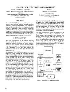
PG L G1 (a)
PVdd
Fig. 1.
II. OVERVIEW The concept of pulsed-Vdd that we propose is illustrated in Fig. 1(a). There is no clock network, so sequencing elements do not have clock inputs. A power supply, denoted by P Vdd , carries periodic negative pulses as shown in Fig. 1(b). The details of P Vdd generation and its distribution will be studied in the future as we continue to develop the concept. The key component is a pulse generator (generator for short), which generates a positive pulse (denoted by pck in Fig. 1(b)) in accordance with each P Vdd pulse. It then triggers a latch to capture input data; thus, the latch in this case behaves as a pulsed latch. A generator may be shared by more than
978-1-4799-1142-4/13/$31.00 ⓒ2013 IEEE
PG output (pck)
Computation time for comb circuit (b)
I. I NTRODUCTION Clock network is a key component in synchronous circuit, and the design of high quality network requires substantial effort. Hybrid clock mesh and tree has become popular to reduce clock skew; however, more area is occupied by network wires when compared to simple clock tree, e.g. two to three times [1]. Clock tree is very susceptible to on-chip process variations [2], which is another reason why mesh structure has become popular. It is well known that clock network is the largest source of power consumption, e.g. about 40% in typical processors [3]. Asynchronous circuit is implemented without clock network but it has its own limitations [4]: about 20% more area is needed, in general, compared to synchronous counterpart, all signals have to be free from hazards, and commercial CAD tools do not support its design. It would be a great benefit if we are able to keep designing synchronous circuits using established design methodologies and CAD tools, but without clock network. The question is how synchronization is maintained.
PG L
(a) A concept of pulsed-Vdd and (b) P Vdd and pck waveforms.
one latch, but we assume an integrated generator and latch in this paper. Consider a fanin gate of latch, G1 in Fig. 1(a). If its output is 0, it is not affected by P Vdd pulse. The output of 1 is affected, but it is restored as the pulse rises (see Fig. 1(a)); note that the input is 0 in this case, which is unaffected. This applies to all CMOS gates, which are inverting logic (even non-inverting gate such as AND is internally inverting). If the gap between rising edge of P Vdd pulse and that of pck is larger than setup constraint of latch, the output of G1 is captured at the rising edge of pck. Computation has to be completed before the next P Vdd pulse as shown in Fig. 1(b), so the width of P Vdd pulse is wasted. III. P ULSED L ATCH D ESIGN A pulse generator is shown on the left of Fig. 2; it outputs a positive pulse pck, which is supplied to a typical latch shown on the right. P Vdd and pck waveforms obtained from HSPICE simulation are shown in Fig. 3 together with the waveforms at two internal nodes of generator, n1 and n2 . Before P Vdd pulse arrives, M1 is turned on and charges C at n1 ; this turns on M3 , so n2 , which is disconnected from n1 , is at 0 voltage. As P Vdd drops at the falling edge of pulse, M2 is turned on, which allows the charges of C to be shared between n1 and n2 , i.e. n1 voltage drops and n2 voltage rises as shown in Fig. 3. Transistors M1 and M3 are made smaller than M2 , so that main charge transfer occurs through M2 in this process, when M1 and M3 are weakly turned on (note that the voltages of P Vdd and n1 are decreasing). At the rising edge of pulse, M2 is turned off and disconnects n1 and n2 ; C is slowly charged again through M1 , which gradually turns on
- 192 -
ISOCC 2013
PVdd
M1 n1 C
M2
Q
n2
pck
pck D
C
pck
M3
Pulse generator
Fig. 2.
A pulse generator and latch.
Fig. 4.
Gap between PVdd and pck pulses
PVdd
Latch
Layout of integrated generator and latch.
PVdd D
pck
Q (a)
Time n1
clk D
n2
Q Time
(b)
Fig. 3. Waveform of P Vdd and pck; n1 and n2 are internal nodes of generator.
Fig. 5. Verifying functionality of (a) pulsed-Vdd circuit as compared to (b) flip-flop circuit.
M3 . A pck pulse is regenerated from n2 waveform by a buffer attached at the output of generator.
Clock skew of pulsed-Vdd circuit was 5.7 ps. The small skew value is another benefit of pulsed-Vdd circuit; it is an understandable consequence because pulses are delivered over Vdd network, which has smaller RC delay. For fair comparison, an effort was put to achieve smaller skew for flip-flop circuit. The resulting clock tree contains 59 buffers and causes 11% larger total wirelength than pulsed-Vdd circuit; Monte Carlo simulation (to account for on-chip process variations on clock tree [2]) of the tree reported 22.3 ps of skew.
IV. E XPERIMENTS A. Generator Design The integrated generator and latch was designed in 32-nm technology. Its layout is shown in Fig. 4; it occupies 27% more area than D flip-flop, but if generator is made external and is shared by two latches, the area sum is estimated to be smaller than that of two flip-flops by 7%. Post-layout HSPICE simulation indicates that pck pulse is 60.6 ps wide, which is wide enough for input data to be safely captured; pck pulse width in turn requires P Vdd pulse at least 53.6 ps wide with rise time of 8.6 ps and fall time of 10.0 ps. The gap between rising edge of P Vdd pulse and that of pck (see Fig. 3) was 9.2 ps; this is larger than 6.4 ps of setup constraint of latch, so latch input can be captured as soon as pck pulse rises as we have addressed in Section II. B. Test Circuit Design and Assessment A test design that performs USB function was selected from OpenCores [5]. Its RTL code was synthesized to yield 5676 gates and 1729 flip-flops; the layout was generated which contains clock tree; the implementation shall be called flipflop circuit. Each flip-flop was then replaced by the integrated generator and latch shown in Fig. 4; the clock tree was removed and periodic P Vdd pulses were applied at one corner of Vdd network; a new implementation shall be named pulsedVdd circuit. To verify whether pulsed-Vdd circuit functions correctly, the input and output waveforms of arbitrarily picked latch were obtained through HSPICE simulation as shown in Fig. 5(a). Corresponding waveforms of flip-flop circuit are illustrated in Fig. 5(b), which functionally match the waveforms of (a).
978-1-4799-1142-4/13/$31.00 ⓒ2013 IEEE
V. S UMMARY We have argued that clock network can be dropped from synchronous circuit. Instead, Vdd network is made to carry periodic pulses, so it is now responsible for synchronization as well as usual power supply. A pulsed latch is employed as a sequencing element; a pulse generator, which is a key component, has been proposed. A great deal of work are left to develop the proposed concept. Consistent supply of pulses over Vdd network is the foremost issue to be investigated. Existence of pulse on power supply implies a potential of charge recycling, which we will study for lower power consumption. A single pulse generator may be shared by more than one latch for the benefit of area. R EFERENCES [1] H. Su and S. Sapatnekar, “Hybrid structured clock network construction,” in Proc. ICCAD, Nov 2001, pp. 333–336. [2] P.-H. Ho, “Industrial clock design,” in Proc. ISPD, Mar. 2009, pp. 139–140. [3] D. Chinnery and K. Keutzer, Closing the Power Gap Between ASIC & Custom. Springer, 2007. [4] J. Sparsø and S. Furber, Eds., Principles of Asynchronous Circuit Design: A Systems Perspective. Kluwer Academic Publishers, 2001. [5] OpenCores, Available http://www.opencores.org/.
- 193 -
ISOCC 2013