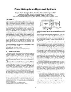
Power Gating and Supply Control for Low Standby Leakage Power of VLSI Circuits* Sewan Heo, Hyung-Ock Kim, and Youngsoo Shin Department of Electrical Engineering, KAIST Daejeon 305-701, Korea Gate leakage and subthreshold leakage currents are two main components that determine standby power consumption of nanometer-scale CMOS circuits. Supply control and combined power gating and supply control are proposed to suppress both components of leakage current. Significant leakage reduction in 45-nm predictive technology model is observed with a set of benchmark circuits. Circuit techniques for designing the proposed schemes are explained. Keywords: gate leakage, low power, power gating, supply control Gate oxide direct tunneling current (gate leakage, for brevity) grows very fast with CMOS technology scaling due to the scaling down of gate oxide. In fact, for CMOS technology of 60nm and below, gate leakage is expected to exceed subthreshold leakage, which is the dominant component of static power consumption in current technology. Thus, suppressing gate leakage, as well as subthreshold leakage, is very important for the design of power-efficient high-performance VLSI circuits such as microprocessors and SoCs. We propose a scheme of supply control, which is conceptually shown in Fig. 1. When the circuit is in active mode, normal supply voltage (Vdd) is applied. When the PMU (Power Management Unit) detects the standby state of the circuit, it steers the supply controller such that the standby supply voltage (Vstandby) is applied to the circuit. Vstandby is considerably lower than Vdd, thereby significantly reducing standby gate leakage since gate leakage is proportional to Vdd4 [1]. Vstandby should be chosen such that, in standby mode, the potential that drives the logic block (denoted as virtual supply voltage (Vddv) in Fig. 1) is larger than the minimum voltage allowed for the storage elements to retain their states, plus some noise margin to guarantee the state retention in the presence of voltage fluctuation. For the flip-flop shown in Fig. 2, with 45-nm predictive technology model [2], we obtain the lowest Vddv through SPICE simulation, while varying the temperature between -50℃ and 100℃, which we assume for the minimum and maximum temperatures, respectively. The plot in Fig. 2 shows that Vddv should be at least 111mV to preserve the states within the range of operating temperature. In practice, the same process needs to be repeated at different process corners to take process variation into account. The supply controller in Fig. 1 can be designed by two MOSFET switches as shown in Fig. 3. Normal Vdd is supplied through M1, which is a pMOSFET switch with high threshold voltage. The choice of high threshold can reduce the subthreshold leakage of M1 (note that M1 is turned off in standby mode). Since, in active mode, Vddv is lower than Vdd due to the voltage drop of M1, circuit delay increases, which implies that M1 sizing is important for circuit performance [3]. The wakeup delay (the delay to switch from standby mode to active, i.e. the delay to turn off M2 and turn on M1) is also dependent on the size of M1. Low threshold voltage is preferred for M2 to make it smaller. Although this choice can induce large subthreshold leakage, its impact can be negligible since M2 turns off in active mode, while most leakage of the circuit is from standby mode. The polarity and the size of M2 are very important for total leakage, since they affect the decision of Vstandby. To gain an understanding of this, we take one of ISCAS'89 benchmark circuits (s344) and, for each size and for each polarity of M2, we simulate the circuit to obtain Vstandby such that Vddv is 111mV. This is done at maximum temperature since we are interested in Vstandby that guarantees Vddv larger than 111mV independent of temperature. Once Vstandby is determined, we again simulate the circuit with fixed Vstandby while we change temperature, to measure the total leakage current for each size and for each polarity. Fig. 4 shows the results for nMOSFET and pMOSFET switches, respectively. Note that at specific Vstandby (i.e. at specific size of M2), Vddv goes up as temperature goes down. This increases the gate leakage of the circuit. However, subthreshold leakage is significantly reduced due to its sensitivity to temperature, which is why the total leakage including both components is decreased.
*
This work was supported by Samsung Electronics.
It is clearly seen from Fig. 4 that nMOSFET induces less leakage current most of the time, thus is preferable for M2. In fact, the total leakage current of the circuit with nMOSFET switch is less than half of the one with pMOSFET switch for most temperatures. This can be understood from the fact that Vstandby is higher for pMOSFET at the maximum temperature (recall that Vstandby is determined at the maximum temperature), which in turn leads to increasingly higher Vddv with decreasing temperature, thus having higher impact on total leakage than for nMOSFET. The size of nMOSFET switch should be chosen such that total leakage is minimized while the area overhead from the switch can be tolerated. Since it can be shown that total leakage approximately correlates with Vstandby, sizing can be done by changing nMOSFET size and monitoring Vstandby from average leakage current of the circuit with Vddv set to 111mV. To validate the proposed supply control scheme, we perform the experiments with a set of circuits extracted from ISCAS'89 and ITC'99 benchmarks. Table I shows the result. The results in the fourth column show that an order of reduction can be achieved by the proposed scheme compared to the original circuits shown in the third column. In standby mode, Vddv is very low, which reduces both subthreshold and gate leakage. However, as shown in Fig. 5, the transistors that are connected to primary inputs of logic '1' are biased to Vdd rather than to Vddv, thus have large gate leakage current. This is because the logic blocks that drive the primary inputs may not exploit supply control (thus, always maintain full logic swing) or may be in active mode. Furthermore, the internal logic still has subthreshold leakage, although it is reduced by Vddv. If we exploit power gating [4] in addition to supply control, input gate leakage and subthreshold leakage can be further reduced. Fig. 6 conceptually shows this scheme of combined supply control and power gating (SC+PG). The combinational logic is connected to GND through a power gating switch, called footer [3], which is controlled by PMU. This scheme works as follows: in active mode, footer is turned on and Vdd drives the logic and storage elements; in standby mode, footer is turned off and the circuit is connected to Vstandby. Once footer is turned off, the potential of internal nodes grows up to Vddv, which reduces gate leakage in the primary inputs and subthreshold leakage in the logic. The combined supply control and power gating has an additional advantage in the use of storage elements. In the conventional power gating, special storage elements need to be used to retain states in standby, which otherwise get lost, at the cost of area overhead. In our scheme, though, we can use the conventional storage elements without change, since their states are retained due to Vddv, which is high enough for state retention even in standby. The fifth column in Table I shows the result with combined supply control and power gating. Compared to the original circuit and to supply control, substantial saving is observed. In the sixth column, we also report the result with MTCMOS scheme [4], which employs both headers and footers. MTCMOS is also efficient for gate leakage as well as for subthreshold leakage, since, by using headers and footers at the same time, the potentials of the nodes, where both switches are connected, are collapsed to about half of Vdd in standby mode, which helps reducing gate leakage. However, employing both headers and footers complicates design process and incurs the overhead in terms in area, routing congestion, and so on. Supply control is less efficient than MTCMOS in terms of leakage saving, but it is convenient to implement especially in standard cell-based design. Combined supply control and power gating is most efficient in leakage saving, with additional advantages over MTCMOS in terms of less design complexity (only footers and no need to use state retention storage elements). The saving from supply control and power gating depends on the states of storage elements in sleep mode, since the leakage of the flip-flip shown in Fig. 2 is different for different states. This implies an interesting problem of state forcing in standby mode, which is one of our future works. [1] [2] [3] [4] [5]
R. K. Krishnamurthy, A. Alvandpour, V. De, and S. Borkar, "High-performance and low-power challenges for sub-70nm microprocessor circuits," in Proc. CICC, May 2002, pp. 125-128. Nanoscale Integration and Modeling Group, "45nm BSIM4 model cards," http://www.eas.asu.edu/~ptm/. S. Mutoh, S. Shigematsu, Y. Gotoh, and S. Konaka, "Design method of MTCMOS power switch for low-voltage high-speed LSIs," in Proc. ASP-DAC, Jan. 1999, pp. 113-116. S. Mutoh, T. Douseki, Y. Matsuya, T. Aoki, S. Shigematsu, and J. Yamada, "1-V power supply high-speed digital circuit technology with multithreshold-voltage CMOS," IEEE JSSC, vol. 30, no. 8, pp. 847-854, Aug. 1995. S. Shigematsu, S. Mutoh, Y. Matsuya, Y. Tabae and J. Yamada, "A 1-V high-speed MTCMOS circuit scheme for power-down application circuits," IEEE JSSC, pp. 861-869, vol. 32, no. 6, June 1997.
Vdd
Vstandby
CLK
CLK D
Supply controller
Q
PMU
V ddv Low Vdd [mV]
CLK
Logic block
Fig. 1 Supply control scheme.
CLK
130 110 90 70 50 -50
0
50
100
Temp. [ C]
Fig. 2 Low Vdd for data retention. Vdd
Vstandby
Vdd
Vstandby
M1
M2
M1
M2
Standby
Standby
Leakage [mA] 30
Standby
25
Vddv
Vddv
20
(a)
(b)
15 10
Fig. 3 Supply control switches.
5 1
Vddv
5 70 9 30 Siz 13 C] e[ -10 17 .[ x] p -50 m Te
Vdd
0
1
5
9 70 Siz 13 30 e[ C] -10 x] 17 .[ p m -50 Te
(a)
Logic block (active)
(b)
Fig. 4 Sizing of supply control switch.
(1)
Vdd M1
Fig. 5 Leakage current in supply control.
Vstandby M2
Standby
PMU Vddv
Table I Comparison of total leakage current (in µA).
Combinational logic
M3
Circuit #gates Orig.
SC
SC+PG
MTCMOS
s344
175
25
2.40 (×10) 0.24 (×104) 0.74 (×34)
s1269
659
95
7.69 (×12)
1.12 (×85) 2.02 (×47)
s3384
1621
247 24.50 (×10)
3.05 (×81) 8.99 (×27)
b03
174
b14
7108
28
2.18 (×13)
0.47 (×60) 1.44 (×20)
935 71.60 (×13) 3.87 (×241) 11.80 (×79)
Fig. 6 Combined power gating and supply control.