Bacsa et al.
Vol. 23, No. 5 / May 2006 / J. Opt. Soc. Am. B
893
Local optical field variation in the neighborhood of a semiconductor micrograting Wolfgang Bacsa, Benjamin Levine, and Michel Caumont Laboratoire Physique des Solides, UMR-CNRS 5477, Université Paul Sabatier, 31062 Toulouse, France
Benjamin Dwir Laboratory of Physics of Nanostructures, Ecole Polytechnique Federal Lausanne, CH-1015-Lausanne, Switzerland Received August 24, 2005; accepted November 24, 2005; posted November 9, 2005 (Doc. ID 64365) The local optical field of a semiconductor micrograting (GaAs, 10⫻ 10 m) is recorded in the middle field region using an optical scanning probe in collection mode at a constant height. The recorded image shows the micrograting with high contrast and a displaced diffraction image. The finite penetration depth of the light leads to a reduced edge resolution in the direction of the illuminating beam while the edge contrast in the perpendicular direction remains high 共⬃100 nm兲. We use the discrete dipole model to calculate the local optical field to show how the displacement of the diffraction image increases with increasing distance from the surface. © 2006 Optical Society of America OCIS codes: 180.5810, 260.1960, 240.6690, 290.1990, 290.2877.
1. INTRODUCTION Optical submicrometer quantitative imaging of structured surfaces has applications in the field of advanced surface inspection, optical tweezers, and photonic crystals. The lateral resolution of lens-based systems is limited by the optical wavelength. Near-field optical techniques use a scanning optical probe smaller than the size of the optical wavelength to overcome this limitation. Lens-based systems as well as most near-field optical techniques illuminate the sample with a nonplanar wave.1 When averaged in time, the superposition of two counterpropagating waves gives rise to a standing wave or fringe pattern. The superposition of the incident nonplanar wave on the object scattered wave leads in general to a complex fringe pattern. Several theoretical simulations and analytical models have been proposed for a few model systems.2–4 Illuminating the sample surface with a collimated monochromatic beam has the advantage that the incident plane wave gives rise to a less-complex standing-wave pattern.4–6 When compared with scanning-force or scanning-tunneling microscopy, optical scanning-probe microscopy has the advantage that optical images can be recorded at larger distances from the surface. Although the lateral resolution is reduced at larger distances, regions of interest can be identified before approaching the probe to the surface to record images with a higher lateral resolution at smaller distances.7,8 Although an ideal planar and opaque surface illuminated with a plane wave creates a perfectly planar reflected wavefront, deviations from this ideal situation are expected to be observable in the case of structured surfaces. The superposition of the incident and reflected waves due to the finite beam width forms a standingwave pattern that is oriented parallel to the surface when averaged in time. Any standing-wave pattern can be re0740-3224/06/050893-4/$15.00
corded using a scanning optical probe in collection mode. The deviations from a planar wave are more pronounced in the neighborhood of the surface. This is so because, for a given image point, the dispersion of the distance to all the contributing points in the surface is larger at smaller distances. This results in a low space coherence, which causes the formation of lateral standing waves. At larger distances, the diffraction image increases in size and overlaps with contributions from neighboring regions, which increases its complexity. Recording diffraction images in the middle field region has the advantage that a high lateral resolution can be maintained, and probeinduced effects are reduced while the diffracted image does not overlap with neighboring regions. Here we aim to understand the observed optical contrast of microgratings in the middle field region using an optical scanning probe in collection mode.
2. EXPERIMENTAL We recorded the local field distribution in a plane parallel to the surface at a constant height of GaAs microgratings 共10⫻ 10 m兲 created by electron-beam lithography (grating grooves depth, 1 m; grove width, 0.7– 1 m). The optical probe and surface were illuminated by a laser beam with an angle of incidence of 50° (wavelength, 669 nm, 10 mW, TE polarization). We used bent metal-coated optical probes (Nanonics Imaging, Ltd., aperture size, 100 nm) and a modified scanning probe instrument (Veeco Instruments, Inc. AFM Model CP-R). We observed that the detected signals were larger by a factor of at least two for TE polarization as compared with TM polarization. We attribute this to the orientation of the induced dipole at the probe edge, which is favorable for TE polarization to scatter light along the axis of the optical fiber. The images were recorded without shear force detection. The in© 2006 Optical Society of America
894
J. Opt. Soc. Am. B / Vol. 23, No. 5 / May 2006
cident beam was inclined toward the bottom in all images. Figure 1(a) shows the schematic of the used geometry: sample surface (S), the plane of incidence (P), the image plane (I), angle of incidence 共␣兲, and optical probe. Figure 1(b) shows the recorded image of the micrograting at a large distance from the sample 共⬎30 m兲. The grating location is indicated by the circle. All experimental images are reproducible and do not depend on a specific optical probe. The image plane is, in general, not parallel to the surface and cuts through the standing wave, created by the incident and reflected planar waves.
Bacsa et al.
The recorded image shows horizontal fringes from the standing waves. The fringe spacing can be used to deduce the tilt angle to correct the substrate orientation. Figure 1(c) shows the same region with the micrograting after tilt correction, which removes the fringes created by the standing wave. This clearly shows that the recorded image depends on the orientation of the image plane with respect to the sample. Apart from the micrograting in the center, other structures (dark regions) and their diffraction fringes are seen on the side. Fine parallel fringes are also seen on the lower side of the location of the micrograting.
3. RESULTS AND DISCUSSION
Fig. 1. (a) Schematic of the reflection collection mode: sample (S), plane of incidence of illuminating beam (P) (TE polarization), angle of incidence 共␣兲, image plane (I), and optical probe. (b) Recorded optical image of micrograting (periodicity, 1.43 m) oriented perpendicular to plane of incidence at a large distance 共⬎30 m兲, and image size 60⫻ 60 m; the incident beam direction is from the lower side and is at an angle of incidence 50°, and the fringe spacing of the standing wave of the incident and reflected beams is 6010 nm. The circle indicates the location of the micrograting. (c) Same scan range and experimental conditions as in (b) after changing the tilt of the image plane.
Figure 2(a) shows a recorded optical image (size 20 m) at a smaller distance 共⬍5 m兲 to the micrograting. We can distinguish a darker region 1 and a brighter region 2. The grating fringes are seen in both regions. The larger distances from the surface than typically used in near-field optics leads to a larger phase difference between the incident and scattered fields. The interference of the two leads to the formation of a diffraction image, which is displaced in the direction of the illuminating beam. The fact that the size of the micrograting is larger than the illumination wavelength modifies the reflected wave locally, and this reproduces the grating structure in the image plane. The two regions seen in Fig. 2(a) are then explained by the superposition of the image formed by the modified reflected wave owing to the presence of the grating and the displaced diffraction image of the grating. Figure 2(b) is an enlargement of the lower right corner of region 2 in Fig. 2(a). The grating structure with horizontal fringes (image size, 6.25 m) is clearly seen. We observe that the sharpness of the edges of the grating is different in the horizontal and vertical directions. The contrast of the vertical edge groove in the horizontal direction is higher. High lateral resolution has been observed earlier7 using the reflection collection mode. Figure 2(c) shows the same micrograting rotated, with the grating fringes in vertical orientation, recording a different image height and keeping the incident beam fixed. The image confirms the high edge resolution perpendicular to the incident beam direction. Displaced diffraction fringes are again superimposed with an image that reproduces the grating structure. Interestingly, we see the horizontal fringes of the grating grooves prolonged into the vertical edge groove. We believe that the finite penetration of the light into the substrate for GaAs at ␥ = 669 nm, which is 500 nm, causes the contrast to spread by 200 nm in the direction of the reflected beam, and this explains why the contrast is larger in the direction perpendicular to the direction of the incident beam. To have a better understanding of the recorded fringe contrast, we have used the discrete dipole model9,10 to calculate the interference pattern of the scattered field from the micrograting with the incident field. The model takes into account of the time-averaged interference of the incident and scattered electric transverse field components of a single dipole and a plane wave. The longitudinal field component has not been included, since the image distance is sufficiently large 共⬎兲. Furthermore, the scat-
Bacsa et al.
Vol. 23, No. 5 / May 2006 / J. Opt. Soc. Am. B
895
see that the model calculation reproduces the diffraction fringes around and below the grating. But we note that the contrast is not entirely reproduced. Region 2 is less clearly seen in the simulated image. We attribute the differences between the experimental observations and the numerical simulations to the fact that we use only a twodimensional distribution of dipoles and neglect the threedimensional structure of the grating. The light penetrates the GaAs substrate, which appears to have the effect to enhance the contrast in the recorded image. The finite penetration of the illuminating beam into the substrate is also expected to have the effect of displacing the diffraction image in the direction of the reflected beam.11 The calculated image gives the possibility of estimating the upper limit for the distance between the surface and the image planes. We deduce an upper limit for the image height of 2 – 3 m from Fig. 3(a). The high lateral resolution 共80 nm兲 suggests that the image height is smaller, and this indicates that the diffraction image is shifted in the lateral direction owing to the finite penetration of the light into the substrate. We conclude that the size of the image that reproduces the grating [Region 2, Fig. 2(b)] is limited by the overlap with the diffracted image, which also depends on the lat-
Fig. 2. Recorded optical image of a micrograting at a smaller distance 共⬍5 m兲 than in Fig. 1(c). (a) Image size 20 m, region 1 is due to diffraction from the micrograting; and region 2 shows the grating fringes. (b) Enlargement of the lower right corner (image size 6250 nm) of image (a). Vertical edges are narrower than horizontal edges. The inset shows a cross-section in the horizontal direction. (c) A rotated micrograting under the same experimental conditions; image size 10 m ⫻ 10 m. The vertical grating edges in the circle are as narrow as in (a) and (b). The arrow indicates the first diffraction fringe from a dust particle.
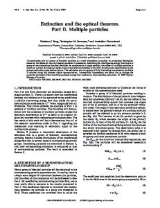
tered field amplitude is several orders of magnitude smaller than the incident field. We therefore neglect the coupling between different discrete dipoles. Higher diffraction orders can be excluded at the image height considered here. The image of the grating is then modeled by the linear superposition of 1180 discrete dipoles. At this stage we have not included the effect of polarization. Figure 3 shows the calculated image contrast at two different image heights (3 and 9). First, we observe that the diffraction image is displaced in the direction of the reflected beam, as observed in the experimental image. The two different heights show that the shift of the diffracted image depends on the image height. Second, we
Fig. 3. Calculated image contrast of the micrograting using 1180 point dipoles: (a) image height 3; the square indicates the location of the grating, and region 1 and region 2 are the same as in Fig. 2; (b) image height 9; the diffraction fringes are displaced in the direction of the illuminating beam. The displacement depends on the image height. The locations of the dipoles are marked by red points.
896
J. Opt. Soc. Am. B / Vol. 23, No. 5 / May 2006
eral shift caused by the finite penetration of the light into the substrate. The separation of the grating image and its diffraction image opens the opportunity to image at a high lateral resolution at a larger distance from the surface where no feedback signal is needed to control the probe in the proximity of the surface. Although the overlap of two images gets smaller with increasing distance from the surface, the reduced lateral resolution at larger distances limits the size of objects that can be observed with high lateral resolution on an opaque substrate.
Bacsa et al.
Wolfgang Bacsa’s current address is Boston University, Electrical and Computer Engineering, 8 Saint Mary’s Street, Boston, Massachusetts 02215. His e-mail address is
[email protected].
REFERENCES 1. 2. 3.
4. CONCLUSIONS We have recorded constant height images of semiconductor microgratings created by electron-beam lithography using reflection-collection-probe, optical-scanning-probe microscopy. Interference fringes due to the tilt of the image plane were corrected by changing the sample orientation. An image of the grating and the superimposed diffracted image are separated in the image plane. The highest observed edge resolution is comparable with the probe aperture size. The finite penetration depth of the light leads to a reduced-edge resolution in the direction of the illuminating beam. Using the discrete dipole model, we have been able to model the diffraction image and explain the displacement of the diffraction image. The larger displacement of the diffraction image observed in the experiment is attributed to the finite penetration of the illuminating beam into the substrate, which is not included in our two-dimensional model. A more detailed simulation of the observed optical contrast will be needed that includes the finite penetration depth of light into the substrate and beam polarization, to fully account for the observed local field variations. The analytic dipole model is able to account for the image displacement and fringe pattern around the micrograting.
4.
5.
6. 7. 8.
9. 10.
11.
D. W. Pohl and D. Courjon, Near Field Optics, NATO ANSI Series (Kluwer, 1993), Vol. 242. S. N. Garcia and M. Nieto-Vesperinas, Optics at the Nanometer, NATO ANSI Series E (Kluwer, 1996), Vol. 319. J. A. Porto, R. Carminati, and J.-J. Greffet, “Theory of electromagnetic field imaging and spectroscopy in scanning near-field optical microscopy,” J. Appl. Phys. 88, 4845–4850 (2000). C. Girard and D. Courjon, “Computing the optical nearfield distributions around complex subwavelength surface structures: a comparative study of different methods,” Phys. Rev. B 42, 9340–9349 (1990). A. Liu, A. Rahmani, G. W. Bryant, L. J. Richter, and S. J. Stranick, “Modeling illumination-mode near-field optical microscopy of Au nanoparticles,” J. Opt. Soc. Am. A 18, 704–709 (2001). N. Umeda, Y. Hayashi, K. Nagai, and A. Takayanagi, “Scanning Wiener-fringe microscope with an optical fiber tip,” Appl. Opt. 31, 4515–4518 (1992). W. S. Bacsa and A. Kulilk, “Interference scanning optical probe microscopy,” Appl. Phys. Lett. 70, 3507–3509 (1997). W. S. Bacsa, “Interference scanning optical probe microscopy: principles and applications,” in Advances in Imaging and Electron Physics, 1st ed., S. Hawks, ed. (Academic, 1999), Vol. 110, pp. 1–19. B. Levine, A. Kulik, and W. S. Bacsa, “Optical space and time coherence near surfaces,” Phys. Rev. B 66, 2334041–233404-4 (2002). B. Levine, M. Caumont, C. Amien, B. Chaudret, B. Dwir, and W. S. Bacsa, “Local optical field in the neighborhood of structured surfaces: phase singularities and Talbot effect,” Technical Proceedings of the Nanoscience and Technology Institute (NTSI, 2004), Vol. 3, pp. 5–9. D. Felbacq, A. Moreau, and R. Smaali, “Goos-Hanchen effect in the gaps of photonic crystals,” Opt. Lett. 28, 1633–1637 (2003).