APPLIED PHYSICS LETTERS 88, 083120 共2006兲
Electrical transport between epitaxial manganites and carbon nanotubes L. E. Hueso,a兲 G. Burnell, J. L. Prieto, L. Granja, and C. Bell Department of Materials Science, University of Cambridge, Pembroke Street, Cambridge CB2 3QZ, United Kingdom
D. J. Kang Nanoscience Centre, University of Cambridge, JJ Thomson Avenue, Cambridge CB3 0FF, United Kingdom and Sungkyunkwan Advanced Institute of Nanoscience and Technology and Center for Nanotubes and Nanostructured Composites, Sungkyunkwan University, Suwon 440-746, Korea
M. Chhowalla Ceramic and Materials Engineering, Rutgers University, Piscataway, New Jersey 08854
S. N. Cha, J. E. Jang, and G. A. J. Amaratunga Department of Engineering, University of Cambridge, Trumpington Street, Cambridge CB2 1PZ, United Kingdom
N. D. Mathur Department of Materials Science, University of Cambridge, Pembroke Street, Cambridge CB2 3QZ, United Kingdom
共Received 14 March 2005; accepted 9 December 2005; published online 24 February 2006兲 The possibility of performing spintronics at the molecular level may be realized in devices that combine fully spin polarized oxides, such as manganites with carbon nanotubes. However, it is not clear whether electrical transport between such different material systems is viable. Here, we show that the room-temperature conductance of manganite-nanotube-manganite devices is only one-half of the value recorded in similar palladium-nanotube-palladium devices. Interestingly, the former shows a gap in the conductivity below the relatively high temperature of 200 K. Our results suggest the possibility of new spintronics heterostructures that exploit fully spin polarized sources and drains. © 2006 American Institute of Physics. 关DOI: 10.1063/1.2170431兴 Spin devices are one of the most sought after elements for the electronics of tomorrow. These devices aim to exploit the spin degree of freedom of the electron, in order to achieve new functionality with respect to conventional electronics. A range of effects has been observed in suitable materials and heterostructures. For example, giant magnetoresistance 共MR兲 is seen in metallic multilayers,1 and tunneling MR is seen in magnetic tunnel junctions.2 These examples exploit the fact that ferromagnets possess spin-polarized electrons. The magnitude of the MR increases when the spin polarization 共P兲 of the ferromagnetic layers is increased,3 where P is defined to be the relative difference between the populations of spin-up and spin-down conduction electrons. This has been investigated experimentally with materials, such as Fe3O4, CrO2 and, more extensively, mixed-valent manganites such as La0.7Ca0.3MnO3.4–7 These compounds have all been argued8 to be half-metallic 共P = 100% 兲 at low temperatures, such that the minority carrier band is empty. If we consider that Co is the best elemental ferromagnet with P = 45%,9 then we can understand the advantage of building spin devices from half-metallic materials. In parallel with these developments in spintronics, the ever-increasing drive toward miniaturization in the semiconductor industry has delivered devices with characteristic length scales that are comparable to the dimensions of some organic molecules.10 To go beyond the silicon roadmap,11 there have been many recent efforts to integrate molecules into electronic circuits. In this molecular electronics apa兲
Author to whom correspondence should be addressed; electronic mail:
[email protected]
proach, many molecules have been tested in order to establish whether they are able to perform basic electronic processes 共such as amplification or rectification兲, or even new and unexpected effects.12 Out of all possible molecular building blocks, carbon nanotubes 共CNTs兲 are among the most studied and have shown the most promising results.13 For example, logic gates14 have been fabricated using roomtemperature transistors based on semiconducting singlewalled CNTs.15 Also, ballistic conduction in nanotubes, which leads to extraordinary properties, offers the possibility of faster devices that consume less power.16 There have been some attempts at integrating spintronics and molecular electronics: Tsukagoshi et al.17 successfully contacted multiwalled CNTs to ferromagnetic Co contacts, and showed a few percent low-temperature MR effect.17 Other groups have obtained similar but inconsistent results.18–21 Our purpose is to show the possibility of electrically connecting a molecule to a magnetic material that shows full spin polarization. We have chosen to work with CNTs and the most promising half-metallic candidate, i.e., a mixed valent manganese oxide 共a manganite兲. If electrical conductivity is possible between such different materials systems, then it may be possible to control electronic spin states in CNTs over distances that are long compared with tunnel junction barrier widths of a few nanometers. Moreover, the diameter of a CNT is much smaller than the lateral dimensions of a typical barrier, suggesting improved performance. Thus, one can envisage large MR effects, as well as the creation of extremely localized sources of spin-polarized electrons, for more challenging applica-
0003-6951/2006/88共8兲/083120/3/$23.00 88, 083120-1 © 2006 American Institute of Physics Downloaded 27 Feb 2006 to 192.167.164.69. Redistribution subject to AIP license or copyright, see http://apl.aip.org/apl/copyright.jsp
083120-2
Hueso et al.
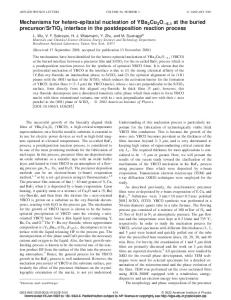
FIG. 1. Scanning electron microscopy photograph of a multiwalled CNT in electrical contact with two manganite lines that act as electrodes for the LSMO-CNT-LSMO devices. Inset: The 3.7 A terraces that are visible in this AFM picture of the LSMO film prior patterning are evidence of good epitaxy, given that the underlying substrate possesses similar terraces due to the vicinal offcut.
tions such as quantum computing.22 From a more fundamental point of view, ferromagnetic contacts may prove a useful probe of spin-charge separation in Luttinger-liquid 共LL兲 materials.23–25 High-quality single-crystal films of La2/3Sr1/3MnO3 共LSMO兲 were grown on commercially available SrTiO3 共001兲 substrates 共Crystal GmbH, Germany兲 by pulsed laser deposition. Details about the sample growth and morphological characterization can be found elsewhere.6 This particular manganite composition was chosen because it is fully spin polarized at low temperature8 and its ferromagnetic properties persist well above room temperature.26 X-ray diffraction and atomic force microscopy 共AFM兲 showed the films are 30 nm thick and fully strained, with unit cell terraces in the surface. Pd was chosen as a control electrode material because it combines a high work function with good wetting properties for nanotubes, leading to a low contact resistance.27 Pd films were grown on SrTiO3 共001兲 substrates by dc sputtering. The Pd resistivity was found to be 20 ⍀ cm at 10 K. Lines of width 1 m and separation 1.5 m were created in the LSMO and Pd films by conventional photolithography and Ar-ion milling. Commercial high-quality multiwalled CNTs 共Iljin Nanotech Co., Ltd., Korea兲 with lengths in excess of 3 m were dispersed on the patterned chips from an ultrasonicated solution 共Fig. 1兲. A total of nine LSMO and 8 Pd working devices were fabricated. We now discuss the electrical transport and magnetic properties of the LSMO films prior to patterning. Metallic behavior was seen from room temperature down to the lowest temperature measured, and a residual resistivity of around 50 ⍀ cm was recorded at 10 K. Ferromagnetic behavior was seen below a Curie temperature of 360 K, and the lowtemperature saturation magnetization is 3.6 B / Mn, just 3% less than the theoretical value of 3.7 B / Mn. Therefore, the manganite films are of the highest possible quality28 ensuring a high P. We first present results for the Pd-CNT-Pd control devices. Nonlinearity in the current-voltage 共I-V兲 characteristics persisted up to room temperature 共Fig. 2兲, and the zerobias anomaly is clearly enhanced at lower temperatures 关Fig. 2 共inset兲兴. Although we find no sign of blocked conductivity
Appl. Phys. Lett. 88, 083120 共2006兲
FIG. 2. A typical I-V characteristic for Pd-CNT-Pd devices. Inset: A typical dI / dV trace showing the development of a zero-bias anomaly at low temperatures.
at low bias at the lowest temperature studied 共4.2 K兲, we attribute this to the fact that we only took data down to 4.2 K. The conductance was found to vary with the characteristic power laws G共T兲 ⬀ T␣共eVⰆ kT兲 and G共V兲 ⬀ V␣共eVⰇ kT兲 with ␣ ⬃ 0.4—not shown. Similar behavior has also been observed in multiwalled CNT-metal samples, and explained using the environmental Coulomb blockade theory.29 Note that we rule out the possibility of conduction pathways via the substrate, since in similar measurements of Pd lines without CNTs, the current is four orders of magnitude smaller 共⬍0.1 nA at 1 V兲. We now turn to our LSMO-CNT-LSMO devices. Our first observation is that all devices measured behave similarly, as do the Pd-CNT-Pd devices. At room temperature, the conductance of the Pd-CNT-Pd devices is around double the conductance of the LSMO-CNT-LSMO devices. Given the resistivities of the device components, the CNT contact resistance in both types of devices 共which we cannot measure in our two-point geometry兲 must dominate. Therefore, the LSMO-CNT contact resistance is roughly double the PdCNT contact resistance. The conductance of the LSMO-CNT-LSMO devices decreases with decreasing temperature, and becomes blocked at ⬃200 K 共Fig. 3兲. This is a remarkably high temperature compared with typical values 共⬃10 K兲13 共Ref. 13兲 in nanotube devices. The gap saturates to ⬃250 meV at very low temperatures 共Fig. 4兲. This blocking energy is remarkably large with respect to typical values 共5–25 meV兲13 共Ref. 13兲 in nanotube devices. At 5 K, the conductance in the highvoltage limit again follows a G共V兲 ⬀ V␣ power law, but with ␣ ⬃ 2.8 in all samples studied 共Fig. 4 inset兲. This value is far from the value of ␣ ⬃ 0.4 obtained earlier for Pd-CNT-Pd devices, and would imply strong repulsive interactions in LL theory. The presence of the gap in all of our LSMO-CNT-LSMO devices suggests that interfacial details are independent of the details of at least the outermost nanotube 共e.g. diameter, chirality, etc.兲. For example, in every case, the crystal lattice mismatch could be poor, and the LSMO surface magnetization30 and thus conductivity suppressed. We note that our device performance is reminiscent of two back-to-
Downloaded 27 Feb 2006 to 192.167.164.69. Redistribution subject to AIP license or copyright, see http://apl.aip.org/apl/copyright.jsp
083120-3
Appl. Phys. Lett. 88, 083120 共2006兲
Hueso et al.
LSMO lines with different widths to achieve different coercive fields, and the use of ultrathin “wetting” layers for reduced contact resistance. The authors thank Peter Littlewood, Maria Calderón, Valeria Ferrari, Ben Simons, Miguel Pruneda, and Emilio Artacho for helpful discussions. This work was funded by the UK EPSRC, the EU Marie Curie Fellowship 共LEH兲, the Royal Society and the NSF 共MC兲. 1
FIG. 3. Typical I-V characteristics at different temperatures for the LSMOCNT-LSMO devices. As the temperature is lowered, a region of blocked conductance appears at low voltages. This can be clearly seen in the dI / dV curves 共inset兲.
back Schottky barriers, but the complexities discussed above preclude the standard analysis. In conclusion, we have established that it is possible to pass an electrical current between a half-metallic oxide and a multiwall CNT. At room temperature, the nanotube contact resistance is only double the value recorded for similar devices with nonmagnetic metallic electrodes made from Pd. Below 200 K, a gap develops in the I-V characteristics and saturates to ⬃250 meV at very low temperatures. Future device improvements include the use of single-wall nanotubes, the incorporation of a gate electrode to permit the carrier density in semiconducting tubes to be varied, the use of
FIG. 4. Estimated values of the blocking energy 共EC兲 extracted from dI / dV for the LSMO-CNT-LSMO devices. The line is a guide for the eyes. Inset: A typical conductance G as a function of the applied voltage V for the LSMO-CNT-LSMO devices at 5 K. The line represents a power-law fit with ␣ = 2.8.
M. N. Baibich, J. M. Broto, A. Fert, F. Nguyen Van Dau, F. Petroff, P. Eitenne, G. Creuzet, A. Friederich, and J. Chazelas, Phys. Rev. Lett. 61, 2472 共1998兲. 2 J. S. Moodera, L. R. Kinder, T. M. Wong, and R. Meservey, Phys. Rev. Lett. 74, 3273 共1995兲. 3 M. Julliere, Phys. Lett. A 54, 225 共1975兲. 4 X. W. Li, A. Gupta, G. Xiao, W. Qian, and V. P. Dravid, Appl. Phys. Lett. 73, 3282 共1998兲. 5 A. Gupta, X. W. Li, and G. Xiao, Appl. Phys. Lett. 78, 1894 共2001兲. 6 M.-H. Jo, N. D. Mathur, N. K. Todd, and M. G. Blamire, Phys. Rev. B 61, R14905 共2000兲. 7 M. Bowen, M. Bibes, A. Barthelemy, J.-P. Contour, A. Anane, Y. Lemaitre, and A. Fert, Appl. Phys. Lett. 82, 233 共2003兲. 8 J.-H. Park, E. Vescovo, H.-J. Kim, C. Kwon, R. Ramesh, and T. Venkatesan, Nature 共London兲 392, 794 共1998兲. 9 R. Meservey and P. M. Tedrow, Phys. Rep. 238, 175 共1994兲. 10 International Technology Roadmap for Semiconductors, 2004 Update. Available at 具http://public.itrs.net/典. 11 N. D. Mathur, Nature 共London兲 419, 573 共2002兲. 12 J. R. Heath and M. A. Ratner, Phys. Today 56, 43 共2003兲. 13 Carbon Nanotubes: Synthesis, Structure, Properties, and Applications, edited by M. Dresselhaus, G. Dresselhaus, and P. Avouris 共Springer, Berlin, 2001兲. 14 A. Bachtold, P. Hadley, T. Nakanishi, and C. Dekker, Science 294, 1317 共2001兲. 15 S. J. Tans, A. R. M. Verschueren, and C. Dekker, Nature 共London兲 393, 49 共1998兲. 16 J. Kong, E. Yenilmez, T. W. Tombler, W. Kim, H. Dai, R. B. Laughlin, L. Liu, C. S. Jayanthi, and S. Y. Wu, Phys. Rev. Lett. 87, 106801 共2001兲. 17 K. Tsukagoshi, B. W. Alphenaar, and H. Ago, Nature 共London兲 401, 572 共1999兲. 18 D. Orgassa, G. J. Mankey, and H. Fujiwara, Nanotechnology 12, 281 共2001兲. 19 B. Zhao, I. Monch, T. Muhl, H. Vinzenbelrg, and C. M. Schneider, J. Appl. Phys. 91, 7026 共2002兲. 20 J.-R. Kim, H. M. So, J.-J. Kim, and J. Kim, Phys. Rev. B 66, 233401 共2002兲. 21 A. Jensen, J. R. Hauptmann, J. Nygård, J. Sadouski, and P. E. Lindelof, Nano Lett. 4, 349 共2004兲. 22 L. Hueso and N. Mathur, Nature 共London兲 427, 301 共2004兲. 23 Q. Si, Phys. Rev. Lett. 81, 3191 共1998兲. 24 H. Mehrez, J. Taylor, H. Guo, J. Wang, and C. Roland, Phys. Rev. Lett. 84, 2682 共2000兲. 25 L. Balents and R. Egger, Phys. Rev. Lett. 85, 3464 共2000兲. 26 A. Urushibara, Y. Moritomo, A. Arima, A. Asamitsu, G. Kido, and Y. Tokura, Phys. Rev. B 51, 14103 共1995兲. 27 A. Javey, J. Guo, Q. Wang, M. Lundstrom, and H. Dai, Nature 共London兲 424, 654 共2003兲. 28 W. Pellier, P. Lecoeur, and B. Mercey, J. Phys.: Condens. Matter 13, R915 共2001兲. 29 A. Bachtold, M. de Jonge, K. Grove-Rasmussen, P. L. McEuen, M. Buitelaar, and C. Schonenberger, Phys. Rev. Lett. 87, 166801 共2001兲. 30 J.-H. Park, E. Vescovo, H.-J. Kim, C. Kwon, R. Ramesh, and T. Venkatesan, Phys. Rev. Lett. 81, 1953 共1998兲.
Downloaded 27 Feb 2006 to 192.167.164.69. Redistribution subject to AIP license or copyright, see http://apl.aip.org/apl/copyright.jsp