IOP PUBLISHING
NANOTECHNOLOGY
Nanotechnology 23 (2012) 175702 (8pp)
doi:10.1088/0957-4484/23/17/175702
Spectrally and spatially resolved cathodoluminescence of nanodiamonds: local variations of the NV0 emission properties L H G Tizei and M Kociak Laboratoire de Physique des Solides, Universit´e Paris-Sud, CNRS-UMR 8502, Orsay 91405, France E-mail:
[email protected]
Received 3 February 2012, in final form 6 March 2012 Published 5 April 2012 Online at stacks.iop.org/Nano/23/175702 Abstract Here we report the spectrally and spatially resolved cathodoluminescence of diamond nanoparticles using focused fast electron beams in a transmission electron microscope. We demonstrate the possibility of quickly detecting various individual colour centres of different kinds on wide areas (several micrometres square) contained in nanoparticles separated by subwavelength distances. Among them, nanoparticles containing one or more neutral nitrogen-vacancy (NV0 ) intensity maxima have been seen, attributable to individual emitters. Thanks to a spatial resolution which is solely limited by charge carrier diffusion in the case of a fast electron (80 keV) setup, the spectra of two individual NV0 emitters separated by 80 nm inside a nanoparticle have been spatially discerned. A shift of the zero phonon line (ZPL) between the two emitters, which we attribute to internal stress, is shown to arise even within the same nanoparticle. Detailed emission spectra (ZPL, phonon lines and Huang–Rhys factor, directly linked to the relaxation energy of the colour centre) in 51 individual NV0 centres have been measured in 39 particles. The ZPL and Huang–Rhys factor are found to be measurably dispersed, while the phonon energies keep constant. (Some figures may appear in colour only in the online journal)
1. Introduction
which is the case of the highly studied nitrogen-vacancy (NV) centres. This makes them serious candidates for quantum computing and cryptography applications. For this reason, detailed knowledge about luminescence of colour centres and their precise characterization in arbitrary environments are fundamental for future developments. For biological marking, the signal to noise ratio of the detected spectra and the sensitivity for single particles are important for marker (colour centre) differentiation and site-specific localization (inside a cell, for example). For single photon sources, spatially resolved optical measurements are necessary in order to address single quantum emitters, from one perspective, and to understand their properties and interactions with a matrix, cavity, or other nearby emitters. As diamond has to be in the form of nanoparticles for most applications
Colour centres in diamond have been studied for decades [1–3]. In more recent years, extensive and thorough studies have focused on individual centres or group of centres in small nanoparticles or bulk [4–11]. This renewed interest has been fuelled by the sheer number of potential applications. Indeed, most of these centres share competitive characteristics compared to other fluorophores such as dyes [12] or quantum dots [13, 14]. Colour centres in diamond have, even at room temperature, high photostability [3] and high quantum yields, can be engineered to not blink in small particles [15], and are biocompatible, making them particularly attractive for biological applications [14, 16]. Moreover, they can be single photon emitters [3, 9–11, 17], 0957-4484/12/175702+08$33.00
1
c 2012 IOP Publishing Ltd Printed in the UK & the USA
Nanotechnology 23 (2012) 175702
L H G Tizei and M Kociak
Figure 1. (a) ADF image of a large field of the sample showing numerous diamond nanoparticles. (b) Composite luminescence image of the same region: the image contains four colours, blue, yellow, green, and red, each corresponding to a different observed colour centre, A band, H3, NV0 , 1.40 eV, respectively. Only a small fraction of the particles shows luminescence. (c) Spectra corresponding to the different colour centres, with the same colour scheme as in (b). The integration time for each spectrum was 50 ms.
then perform a detailed analysis of the spectra of different NV0 (neutral NV) centres within individual nanoparticles. We evidence how the ZPL emission wavelength can shift from one site to another on a deep subwavelength scale, while the phonons’ replicas basically keep the same energy. Finally, performing an analysis on 51 individual NV centres, we evidence a marked change of the so-called Huang–Rhys S factor—a quantity closely related to the relaxation energy of the defect.
and/or individual centres have to be isolated, high spatial resolution, possibly subwavelength, techniques have to be used. Moreover, spectral resolution is also demanded if the source must produce indistinguishable photons [18], for material characterization purposes [19, 20] or to unveil fundamental physical effects [21]. Recent developments in stimulated emission depletion microscopy (STED) [5, 22] have allowed the observation of single emitters down to 5 nm resolution. Unfortunately, this latter technique is not genuinely a spectroscopic technique. The detailed information that can be extracted from spectra, usually formed by a zero phonon line (ZPL) followed by phonon replicas, is thus not recovered. Photoluminescence (PL) [1–3] and cathodoluminescence (CL) [20, 23–25] have been used extensively in the past. The PL has been shown to identify individual centres diluted on a micrometre scale [3], but the technique is intrinsically diffraction limited. CL studies reported high throughput spectroscopic detection of colour centres, but the ensemble average might lead to a blurring of individual centres’ fine structures. Subwavelength spectral characterization of individual centres has never been reported to the best of our knowledge. Colour centres are punctual defects, created by the presence of substitutional or interstitial atoms or vacancies in different configurations. For example, the NV centres are formed by a substitutional nitrogen (N) atom bonded to a vacancy (V). Defects in semiconductors can drastically change their mechanical [26, 27] and electrical properties [28]. Cathodoluminescence has been extensively used to study defects in semiconducting materials, such as dislocations [29, 30] and boron doping atoms [31]. The particular emission signature of dislocations in diamond has also been studied using cathodoluminescence [24, 25]. Here, we report subwavelength spatially and energy resolved measurements of colour centres in nanodiamond particles using a cathodoluminescence system in a scanning transmission electron microscope (STEM). With this system, hyperspectral cathodoluminescence images have been acquired. By making use of the combined spatial and spectral resolutions of our setup, we demonstrate the measurement of the full spectra for two different types of individual centre separated by less than 50 nm in a single nanoparticle. We
2. Materials and method Measurements have been performed at around 150 K in a scanning transmission electron microscope (STEM) VG 501 HB operated at 80 kV (unless otherwise stated) and equipped with a cold field emission gun. Typical currents of 1 nA have been used. Typical probe sizes used have been 1 nm. In a hyperspectral imaging cathodoluminescence experiment, the fast electron beam is scanned over the sample of interest, which has to be thin enough (typical thickness below 200 nm) to be electron transparent. At each beam position, two different kinds of signal are collected in parallel. Firstly, signals related to the structure of the sample can be collected, the bright field signal (BF) at small scattering angle, and the high angle annular dark field (HAADF) signal at high scattering angles. Of particular interest is the HAADF signal, which is to a good approximation proportional to the projected mass under the beam. Synchronously with those, a cathodoluminescence spectrum, collected though a parabolic mirror and sent to an optical spectrometer is acquired. At the end of the scan, BF and HAADF images and a 3D data set, constituted by a spectrum in each pixel, can be reconstructed. This later can be processed a posteriori to produce intensity or more complex maps (as explained below). It is worth noting the capabilities and potentials of multisignal acquisition, which permits the correlation of spectral changes to structural variations and the tracking of spectral evolution as a function of position, as exemplified in figure 1. The spectrometer was calibrated using a mercury lamp. In all experiments shown, the dispersion has been set to 0.55 nm/pixel; this limits our absolute error in wavelength to 0.6 nm. The CCD was coupled to the scanning system 2
Nanotechnology 23 (2012) 175702
L H G Tizei and M Kociak
of the electron microscope (in-house electronics) allowing the acquisition of spectrum images (that is, an image in which each pixel contains a full CL spectrum), following [32]. Spectrum image acquisition is important not only because it offers spatial and spectral resolution in the same data set, but also because it allows the tracking of the evolution of spectral features as a function of position. This enables the full-colour characterization of individual diamond nanoparticles and the observation of cathodoluminescence spatial variation within them. Moreover, as will be further explained, it opens the possibility of measuring physical quantities of colour centres separated by less than 50 nm within the same particle. The experimental setup has been recently shown to be capable of similar measurements in single GaN/AlN quantum emitters in nanowires [33] and to possess remarkable photon-collection efficiency. The resolution of the experiment, of the order of 4 nm in [33], was shown to be mainly limited by the charge carrier diffusion length, and not by the probe size or probe broadenings, which are smaller than 1 nm at the high velocity of the electrons delivered by a STEM. It should be remarked that this would not be necessarily true in a scanning electron microscope setup (lower accelerating voltage results in a larger probe diameter and smaller penetration depth). Two samples have been used: (a) one with polycrystalline diamonds (compressed in a mortar) with typical sizes above 100 nm (Aldrich), hereafter named A, and (b) one with monocrystalline submicrometre (below 300 nm) diamond particles, hereafter named B (Microdiamant 0.250 µm powder). No special treatment has been performed, other than dilution in pure water and dispersion on holey carbon films placed on a 3 mm copper grid.
and the 1.40 eV centre related to nickel at 885 nm [2] (blue, yellow, green and red spectra, respectively, in figure 1(c)). The blue band is probably the so-called A band, which can be associated with luminescence from dislocations [2]. An accepted model for the H3 centre is a vacancy bound to two substitutional nitrogen atoms [2]. The spatial distribution of the intensity luminescence of each centre has been mapped in a false colour image (figure 1(b)), in which the colour code is the same as in figure 1(c) for individual spectra, showing luminescence from one or more centres present in different NPs. The intensity maps have been constructed by summing the intensity in each pixel within the observed emission range of each centre in the spectrum image (subtracting the background, depending on the case, by interpolating power law curves). The used wavelength ranges have been: 380–500 nm (blue, blue band); 500–560 nm (yellow, H3 centre); 570–700 nm (green, NV0 ); and 880–910 nm (red, 1.40 eV centre). As we can directly compare the electron images (BF and ADF) to the luminescence map, we see that, markedly, only a small fraction of the NPs (a few tens, or roughly 10% of the total) are luminescent. This is expected, as no heat or radiation treatment (apart from high energy electron exposure during imaging) has been employed to create or activate colour centres in our samples, leaving only naturally occurring ones active. This experiment demonstrates this setup’s capabilities to detect and discern single particles containing different colour centres over a wide area with fast acquisition times and high spectral resolution. It is important to note that it is the spectral resolution that prevents us from mistaking the tail of the H3 centre to higher wavelengths with an NV0 signal. Moreover, for a specific emission line, the incidence of luminescence is sparse, as depicted in figure 1. This is expected in raw materials where the density of colour centres is smaller than the inverse of an NP volume (less than one colour centre per particle). It is also a strong indication that the emission comes from individual or few colour centres (this point will be discussed in detail later on). In the case of NV centres, we have noted dispersion on the intensity of emission of different nanoparticles. This is most likely related to the luminescence mechanism: a fast electron beam creates charge carriers that diffuse in a volume of (λd )3 where λd is the diffusion length of the charge carrier. If a colour centre stays within this volume, charge carriers recombine radiatively. As the number of created charge carriers increases with increasing thickness of the NP along the electron path, the signal of an individual centre is dependent on the exact geometry of the nanoparticle, which can vary from one to another.
3. Results and discussion Our experiments can be separated into three groups which demonstrate different points: (1) section 3.1 describes large field of view analysis, which focuses on the fast identification of distinct colour centres; (2) section 3.2 depicts the presence of localized cathodoluminescence intensity maxima that can be attributed to individual centres, and the statistics of these maxima in the case of NV0 centres; (3) finally, section 3.3 is dedicated to the analysis of the variation of the emission properties of individual NV0 centres (emission wavelength, phonon replicas and S factor) within and between particles. 3.1. Large field of view analysis To begin with, we have performed experiments over large fields of view (3–5 µm). In figure 1(a) we show the annular dark field (ADF) image of a 3.3 µm wide region of a sample containing a high density of diamond nanoparticles (NPs) of sample B. In this field, containing a few hundred NPs, a 128×128 (26 nm wide pixels) cathodoluminescence spectrum image, with 50 ms acquisition time per pixel and a total acquisition time of roughly 14 min, has been acquired. In this spectrum image four different emissions can be readily identified: a band around 400 nm, the H3 centre around 500 nm, the NV0 with a zero phonon line (ZPL) at 575 nm
3.2. Spatially localized intensity maxima: isolation of individual colour centres within individual nanodiamond In figures 2(a) and (b), we show the HAADF image and an overall spectrum of a diamond NP. In this particular example, luminescences from three different colour centres (H3, NV0 and 1.40 eV) are observed. The resulting maps for the 1.40 eV and the NV0 centres are shown in figures 2(c) and (d), 3
Nanotechnology 23 (2012) 175702
L H G Tizei and M Kociak
Figure 2. (a) HAADF image of a single diamond particle from sample A. (b) Typical spectrum of a region containing the NV0 centre. The marked regions show where the intensity was integrated (with background subtraction by interpolation) to construct the maps of the NV0 (green, (c)) and the 1.40 eV (yellow, (d)) emission intensities. (c)–(d) Intensity maps of the NV0 and the 1.40 eV colour centres. Note that the maxima of each emission do not occur at the same position within the same particle (crosses in the maps indicate the maximum of the NV0 emission). This indicates they do not have the same physical origin.
constant thickness is proved by the HAADF signal. Also, we have performed complementary thickness measurements using a standard treatment of the low loss electron energy loss spectroscopy (EELS) spectra [34]. Concerning the intensity in the same particle, this is coherent with experiments performed on bulk diamond [3], in which different centres have similar intensities. Regarding the number of particles that emit, different experiments [15, 35] have shown that only a small fraction of diamond nanoparticles emit in samples with small density of defects. This indication, associated with our current spectral and spatial resolution, opens the way to perform experiments envisaging the measurement of physical properties of single centres at close proximity. In particular, our typical spectra allow the measurement of the emission lines associated with phonon processes and the quantification of the Huang–Rhys factor, S (a quantity directly related to the relaxation energy [19]), as will be described in section 3.3.
respectively, with the integrated area shown in yellow and green in figure 2(b), respectively. For the 1.40 eV centre, the total intensity is distributed throughout the NP, being more intense at its centre, where it is thicker (maximum marked by circles), as deduced from the HAADF signal. In contrast, the NV0 emission is localized only at a specific position in the NP (marked by a cross). The maxima of both emissions do not occur at the same position (separated by (47 ± 8) nm), showing that they do not have the same origin. The occurrence of localized maxima of the NV0 emission along with the observation that only a small fraction of particles emits light has led us to the hypothesis that we are observing single or few defects. These maxima have been characterized in 39 different NPs of both samples. The NV0 emission is seen to be localized at single or multiple regions. For sample A, 15 particles have been measured, of which seven had one maximum, six had two, and two had three or more. For sample B, all 24 had a single localized maximum (two centres have been measured twice). This indicates that the natural occurrence of NV0 is smaller in sample B. As an example of these particles, in figure 3 we show an HAADF image and the NV0 intensity after the H3 background subtraction (performed by interpolation). The full-width at half-maximum (FWHM) of the emission region is 70 nm, while emission can be detected in a 170 nm circle. The presence of localized maxima inside the same particles, the high number of particles with a single maximum and the high number of particles without the NV0 emission indicate that we are probably observing the luminescence originating from single centres. In addition, the intensity at two different maxima in the same particle (such as in figure 4, described later) have the same amplitude, which would be expected if our hypothesis were true and the particles approximately had the same local thickness. That each nanoparticle has a
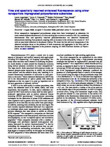
3.3. Emission properties and local variations: ZPL, phonon replicas and Huang–Rhys factor The emission spectrum of the NV0 centre (in figure 4 a background subtracted spectrum with 25 s exposure time is shown) is constituted by a ZPL and three discernible phonon-related emission lines. The ZPL typically occurs at 575 nm (2.156 eV), but we have observed shifts to higher and lower energies, as described later on. The three phonon lines are observed at 2.112, 2.063 and 2.017 eV (averages over the experiments described later on) with some variations also. The energies associated with these peaks (relative to the ZPL) are 44 meV, 90 meV and 139 meV, respectively (marked P1, P2 and P3 in figure 4). These energies have been measured by carefully fitting the emission spectra with Gaussian peaks. An example of a fitted spectrum is shown in figure 4. Similar 4
Nanotechnology 23 (2012) 175702
L H G Tizei and M Kociak
Figure 4. NV0 emission spectrum (black line) with background subtracted with the ZPL at 574.6 nm and the phonon associated lines at 586.1 nm (P1), 600.4 nm (P2) and 615.4 nm (P3). The integration time for this spectrum was 25 s. The fitted spectrum (six Gaussian peaks) is shown in blue. Each individual fitted peak is shown in red. The blue and red curves have been shifted to facilitate visualization.
in previous experiments on naturally strained nanoparticles only ensemble spectra were recorded, resulting, at best, in a splitting of the ZPL and at worst in a complete blurring of the phonon replicas. Thanks to the achieved spatial and spectral resolutions, such splitting and blurring can indeed be attributed to an averaging effect on shifted spectra, and not to a splitting and blurring arising at the single NV level. Also, it shows that, even in a single nanoparticle with two individual emitters, a shift in energy can be present. The intensity map of the NV0 centre is shown in figure 5(c), where two maxima can be seen separated by approximately 80 nm. This and the ZPL shift can be more clearly seen in a line profile (figure 5(d), a projection of the spectrum image along the line shown in figure 5(c) between the two centres), in which the ZPL is observed to shift as a function of position (the maxima are marked by two arrows). We note that the phonon replicas shift in absolute value but their energy separations from their particular ZPL stay the same. Further evidence of the presence of two independent emitters is shown by multiple linear regression of the data using the two spectra in figure 5(b) as independent variables. The results show that the full spectrum image is well fitted by two components corresponding to spectra of figure 5(b) (added to a constant background) and that the coefficient of each component is peaked in spatially separated regions (figures 5(e) and (f)). These regions are also where the intensity maxima occur. This indicates that the luminescence originates from two different sources, which we attribute to two spatially separated individual NV0 centres. In addition to the change in the ZPL line wavelength, it can be seen that the intensity ratio between the ZPL and the phonon associated lines at lower energies is not the same in both centres (figure 5(b)). It is known [19] that the ratio between the ZPL and the total intensities is linked to the S factor (S = − ln(I0 /Itotal )). For these two centres, the measured S values are S1 = (3.2 ± 0.2) and S2 = (2.9 ± 0.2). The variation of light transmission as a function of wavelength in our detection setup is smaller than our experimental error (around 1%) in the relevant wavelength range. The observed S variation shows that the physical properties of each emitter
Figure 3. (a) HAADF image of a single diamond particle from sample B. (b) NV0 emission intensity map constructed as in figure 2. The intensity is peaked at a single maximum of 70 nm FWHM within the particle and not correlated to the HAADF signal (that is, thickness). The presence of particles with a single emission maximum indicates the detection of single colour centres.
energies have been measured previously for these three peaks using cathodoluminescence and photoluminescence on bulk samples [20, 23, 36]. However, the exact origin of these phonons is not perfectly clear. These lines may be related to local vibration modes (LVM), which appear due to the introduction of the defect. Moreover, it is known that an acoustic mode at 75 meV and an optical mode at 160 meV [19] contribute to the phonon spectra of NV centres. However, we did not find evidence of peaks at these energies in our spectra. Recent simulations have shown that an LVM exists at 35 meV for the NV− (charged NV) centre, but it is not active due to symmetry considerations [21]. As previously stated, in sample A we have observed the existence of particles containing more than one NV0 intensity maximum that can be spatially isolated, which we attribute to more than one centre. In figure 5, we show an example of such particles (ADF on figure 5(a)). The ZPL from regions centred on each maximum (spectra in figure 5(b)) can be seen to be slightly different (λ1 = (573.5 ± 0.6) nm and λ2 = (574.6 ± 0.6) nm). This shift may be attributed to strain differences between the two positions [1, 37]. ZPL shifts in bulk diamond due to natural strain (not externally applied) have been observed [37]. It is worth noting that 5
Nanotechnology 23 (2012) 175702
L H G Tizei and M Kociak
Figure 5. (a) ADF image of single diamond particle from sample A. The spectrum image shown in (c)–(f) has been acquired in the rectangle marked in white. (b) Spectra of the NV0 emission acquired in 200 ms (Noise in the data has been reduced by principal component analysis PCA [38].) centred at both emission maxima. A small shift in emission wavelength is observed, along with a change in the ZPL/phonon lines intensity ratio. (c) Intensity map of the NV0 emission (integrated from 565 to 725 nm). (d) Projection along a line (shown in (c)) of the spectrum image, with the spatial position along the x axis and the emission wavelength along the y axis. The intensity maxima are marked by arrows in (c) and (d). The ZPL and associated phonon lines can be clearly seen, as well as the shift between the two centres. (e), (f) Maps of the coefficients of the multiple linear regression performed for the two independent components (shown in (b)). The colour scale range is the same in (e) and (f). The two components are spatially separated, evidence of the presence of two sources.
change. This could be related to strain effects, as in the ZPL shift observed. The strain effect (or any other possible cause) at the origin of the S change is directly linked to a local change in oscillator strength of the phonons that has not been reported previously to the best of our knowledge. With this in mind, we have carefully fitted the emission spectra of 37 emitters in 28 particles, using multiple Gaussians, in order to measure their phonon associated peak wavelengths and the S factors. A detailed fitted spectrum is shown in figure 4. First of all, this procedure allowed us to measure the energy associated with processes resulting in luminescence in the first, the second and the third phonon-related peaks (figures 6(a)–(c)), that is the energy differences between the ZPL and the phonon peak. These differences in energy do not change substantially (within our experimental errors) as can be seen in the histogram of figure 6(d). The standard deviations for the ZPL energy (EZPL ), the first peak energy (EP1 ) and the first phonon energy (E1 = EZPL − EP1 ) are σZPL = (2.6 ± 0.3) meV, σEP1 = (2.7 ± 0.2) meV and σE1 = (1.8 ± 0.2) meV, respectively. This indicates that the phonon-related processes are roughly the same and that it is the initial state that changes. The fitted curves also allow us to measure the S factor of each emitter. The measured values vary from 2.3 to 4 with typical errors around 0.2 (limited by the subtraction of the background due to the H3 centres).
Once again, the S factor is related to the relaxation energy of the centre [19]. We are not aware of such systematic study of the S factor variation, because published results on the subject are sparse, and usually give a value between 2 and 3 on bulk materials [19, 39]. This variation of the S factor is probably linked to modifications in the local environment of the centre, which could be induced by strain, size or surface effects. The measured values for S and the ZPL for all centres measured are shown in figure 6(e). The presence of two NV0 cathodoluminescence intensity maxima within the same particle with different physical properties is a strong indication for the identification of individual NV0 centres. This is also strongly supported by the fact that we observed two different, well resolved, spectra at both positions. We should point out that the discrimination of two colour centres separated by 80 nm is only possible due to the small carrier diffusion length in these nanoparticles, which prevents the excitation of distant centres, associated with the small thickness of the sample, which limits the fast electron beam spread to small volumes. Low loss EELS, using an estimate for the electron mean free path [34] at 80 kV, shows that particle thickness is fairly uniform within a particle and varies from particle to particle between 30 and 160 nm (in 15 measured particles). 6
Nanotechnology 23 (2012) 175702
L H G Tizei and M Kociak
Figure 6. (a)–(c) Phonon energies for the first three phonons (ZPL energy minus the respective phonon peak replica). (d) Histogram of the ZPL and phonon associated emission energies. The reproducibility of the measured energies (given our experimental errors) is the evidence that the phonon band does not change much. (e) S factor value and ZPL wavelength for measured emitters (error bars for the wavelength represent the statistical fit error; absolute errors for the wavelength measurements are 0.6 nm or about 2 meV in the measured range).
centres. Furthermore, our data indicates that we are possibly capable of detecting single colour centres in diamond and of differentiating them by measuring physical properties such as the ZPL emission wavelength, phonon replica emission wavelength and S factor with sub-100 nm resolution and 1 nm sampling. This, we stress, is possible only due to the capability of fast acquisition of spectrally and spatially resolved data. At first sight one would expect that similar results could be achieved in a SEM system, which nowadays can form electron probes significantly smaller than 10 nm. What probably makes for most of the contrast between the present results and previously published ones is the electron speed. This quantity is much smaller in SEM, which leads to a broadening of the probe within the sample and to heating effects, due to the absorption and diffusion of the incoming electrons in the true body of the sample. Thus, extension of our work to regular and widespread SEM might be possible with the condition of using the highest accelerating voltage and of the thinnest samples. CL spectral imaging thus emerges as a potential affordable alternative to pure optical methods to study individual emission centres with yet better spatial resolution. Even then, to the best of our knowledge, characterizations such as present here have not been performed in individual diamond nanoparticles containing themselves one or a few individual different colour centres. These measurements may aid the characterization of colour centres and their development as single photon sources.
3.4. Emission time stability Lastly, a final important point about these experiments is the stability of the NV0 emission under electron irradiation. We have performed experiments with 100 kV electrons that show that the NV0 centres are not stable, with luminescence ceasing suddenly (not continuously) and uncontrollably after a few minutes of exposure. On the other hand, most of the NV0 are stable under 80 kV electrons even after 2–3 h of exposure. The same is true at 60 kV. This property allows the acquisition of high quality data, which would be unfeasible with unstable colour centres. Also, 60 keV is large enough to obtain an electron beam well below the 1 nm size, that will not significantly broaden or be absorbed by the relatively thin nanoparticles investigated.
4. Conclusions We have explored the capabilities of cathodoluminescence in a STEM for the imaging of colour centres in diamond nanoparticles with high spatial and spectral resolutions. This high spatial resolution is only available because of the small thickness of the particles. The high collection efficiency of the system allows the fast acquisition (∼50 ms) of full spectra, enabling the full-colour imaging of diamond with high spatial resolution (in the nanometre range). This permits one to readily differentiate nanoparticles containing different colour 7
Nanotechnology 23 (2012) 175702
L H G Tizei and M Kociak
Finally, the ZPL wavelength, phonon energies and S factor measurements open ground to further model the physics of phonons/defects in diamond and more complex materials (such as polar covalent solids, e.g. BN [40] and SiC).
[15] Bradac C, Gaebel T, Naidoo N, Sellars M J, Twamley J, Brown L J, Barnard A S, Plakhotnik T, Zvyagin A V and Rabeau J R 2010 Nature Nanotechnol. 5 345 [16] McGuinness L P et al 2011 Nature Nanotechnol. 6 358 [17] Babinec T M, Hausmann B J M, Khan M, Zhang Y, Maze J R, Hemmer P R and Loncar M 2010 Nature Nanotechnol. 5 195 [18] Santori C, Fattal D, Vuckovic J, Solomon G S and Yamamoto Y 2002 Nature 419 594 [19] Davies G 1981 Rep. Prog. Phys. 44 787 [20] Burton N C, Steeds J W, Meaden G M, Shreter Y G and Butler J E 1995 Diamond Relat. Mater. 4 1222 [21] Abtew T A, Sun Y Y, Shih B-C, Dev P, Zhang S B and Zhang P 2011 Phys. Rev. Lett. 107 146403 [22] Han K Y, Willig K I, Rittweger E, Jelezko F, Eggeling C and Hell S W Nano Lett. 9 3323 [23] Robins L H, Cook L P, Farabaugh E N and Feldman A 1989 Phys. Rev. B 39 13367 [24] Yamamoto N, Spence J C H and Fathy D 1984 Phil. Mag. B 49 609 [25] Pennycook S J, Brown M L and Craven A J 1980 Phil. Mag. A 41 589 [26] Han X D, Zhang Y F, Zheng K, Zhang X N, Zhang Z, Hao Y J, Guo X Y, Yuan J and Wang Z L 2007 Nano Lett. 7 452 [27] Tizei L H G, Craven A J, Zagonel L F, Tenc´e M, St´ephan O, Chiaramonte T, Cotta M A and Ugarte D 2011 Phys. Rev. Lett. 107 195503 [28] Yu Y P and Cardona M 2005 Fundamental of Semiconductors (Berlin: Springer) [29] Ponce F and Bour D P 1997 Nature 386 351 [30] Brooksby J C, Mei J and Ponce F A 2007 Appl. Phys. Lett. 90 231901 [31] Barjon J, Desfonds P, Pinault M-A, Kociniewski T, Jomard F and Chevallier J 2007 J. Appl. Phys. 101 113701 [32] Jeanguillaume C and Colliex C 1989 Ultramicroscopy 28 252 [33] Zagonel L F et al 2011 Nano Lett. 11 568 [34] Egerton R F 1996 Electron Energy-Loss Spectroscopy in the Electron Microscope (New York: Plenum) [35] Rabeau J R, Stacey A, Rabeau A, Prawer S, Jelezko F, Mirza I and Wrachtrup J 2007 Nano Lett. 7 3433 [36] Iakoubovskii K, Adriaenssens G J and Nesladek M 2000 J. Phys.: Condens. Matter. 12 189 [37] Faraon A, Barclay P E, Santori C, Fu K-M C and Beausoleil R G 2011 Nature Photon. 5 301 [38] de la Pe˜na F, Berger M-H, Hochepied J-F, Dynys F, Stephan O and Walls M 2011 Ultramicroscopy 111 169 [39] Davies G 1979 J. Phys. C: Solid State Phys. 12 2551 [40] Jaffrennou P, Donatini F, Barjon J, Lauret J-S, Maguer A, Attal-Tretout B, Duscastelle F and Loiseau A 2007 Chem. Phys. Lett. 442 372
Acknowledgments We thank L F Zagonel and F Treussart for insightful discussions. The authors acknowledge financial support from the European Union under the Framework 6 program under a contract for an Integrated Infrastructure Initiative, reference 026019 ESTEEM, and French ANR (1010 BLAN 1016 ‘HYNNA’).
References [1] Davies G and Hamer M F 1976 Proc. R. Soc. A 348 285 [2] Zaitsev A M 2001 Optical Properties of Diamond (Berlin: Springer) [3] Gruber A, Dr¨abenstedt A, Tietz C, Fleury L, Wrachtrup J and von Borczyskowski C 1997 Science 276 2012 [4] Weber J R, Koehl W F, Varley J B, Janotti A, Buckley B B, Van de Walle C G and Awschalom D D 2010 Proc. Natl Acad. Sci. 11 8513 [5] Rittweger E, Han K Y, Irvine S E, Eggeling C and Hell S W 2009 Nature Photon. 3 144 [6] Kolesov R, Grotz B, Balasubramanian G, St¨ohr R J, Nicolet A A L, Hemmer P R, Jelezko F and Wrachtrup J 2009 Nature Phys. 5 470 [7] Dolde F, Fedder H, Doherty M W, N¨obauer T, Rempp F, Balasubramanian G, Wolf T, Reinhard F, Hollenberg C L, Jelezko F and Wrachtrup J 2011 Nature Phys. 7 459 [8] Zhao N, Hu J-L, Ho S-W, Wan J T K and Liu R B 2011 Nature Nanotechnol. 6 242 [9] Aharonovich I, Castelletto S, Simpson D A, Su C-H, Greentree A D and Prawer S 2011 Rep. Prog. Phys. 74 076501 [10] Brouri R, Beveratos A, Poizat J-P and Grangier P 2000 Opt. Lett. 25 1294 [11] Treussart F, Jacques V, Wu E, Gacoin T, Grangier P and Roch J-F 2006 Physica B 376 926 [12] Fu C-C, Lee H-Y, Chen K, Lim T-S, Wu H-Y, Lin P-K, Wei P-K, Tsao P-H, Chang H-C and Fann W 2007 Proc. Natl Acad. Sci. 3 727 [13] Ehlert O, Thomann R, Darbandi M and Nann T 2007 ACS Nano 2 120 [14] Alivisatos P 2004 Nature Biotechnol. 22 47
8