8.3
Physical Design Methodology of Power Gating Circuits for Standard-Cell-Based Design Hyuk Kim, Iksoo Eo
Hyung-Ock Kim, Youngsoo Shin Department of Electrical Engineering, KAIST Daejeon 305-701, Korea
Electronics and Telecommunications Research Institute (ETRI) Daejeon 305-350, Korea
ABSTRACT
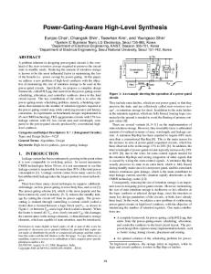
T Vdd
The application of power gating circuits to semicustom design based on standard-cell elements is limited due to the requirement of customizing cells that are tailored for power gating or the requirement of customizing physical design methodologies for placement and power network. We propose a new power network architecture that enables use of conventional standard-cell elements. A few custom library elements are developed wherever needed, including output interface circuits and data retention storage elements. A novel method of current switch design is also described. The proposed methodology is applied to ISCAS benchmark circuits, and also to a commercial Viterbi decoder with 0. I 8,um CMOS technology, Categories and Subject Descriptors: B.7. 1 [Integrated Circuits]: Types and Design Styles-VLSI
a E
c:ombinational
logic. crus
L;
Output hauig _
.
,VSS
.
i- Footer
-landby
Figure 1: Power gating circuits. current in the blocks that are connected to the outputs, as well as logical errors in the outputs themselves. This can be alleviated by employing an interface circuit with the capability of preserving the logic during standby mode. Since storage elements lose their states in standby mode, altemative elements, which are capable of data retention, must be used. Sizing of current switch is critical in terms of performance, area, and leakage current [2]. These design issues specific to power gating, some of which call for tool support, make the application of power gating to semicustom designs difficult, especially to those based on standard-cell elements. In addition to these issues, a physical design methodology needs to be tailored. A cell library specific to power gating needs to be designed to accommodate the requirement of additional power networks [1], [3]. The location of current switches and power-gating specific cells such as data retention storage elements is limited [4], which severely constrain the placement of logic cells. These problems are, in essence, due to the heterogeneous requirement on power networks. As an example, Figure 1 shows that footers need V,, and VS,,; logic cells are powered by Vdd and Vss,; data retention storage elements require all three power networks; output interface circuits need Vdd and Vs. In this paper, we propose a new power network architecture, which enables use of conventional standard-cell elements without modification. A design method of current switch is proposed and the impact of its substrate biasing is studied. We address a layout methodology for current switch, which can trade-off area overhead with power network design. A design method of current switch is proposed in terms of substrate biasing and its placement. We propose a new output-holding circuit and compare to previous works. The proposed methodology is applied to ISCAS benchmark circuits, and also to a commercial Viterbi decoder with 0.18,um CMOS
General Terms: Design Keywords: Power gating, low power, leakage current
1. INTRODUCTION Subthreshold leakage current grows exponentially with every process generation, due to the scaling down of the threshold voltage. Many circuit level approaches have been proposed including input vector control, power gating, dynamic voltage scaling, body biasing, and so on. Power gating uses a current switch to cut off a circuit from its power supply rails during standby mode, and has been widely used in the semiconductor industry to reduce subthreshold leakage. Power gating is realized by placing a current switch, called a footer, in series with a logic block, as shown in Figure 1. A header, which is a PMOS switch placed between Vdd and logic block, can also be used. When the power management unit (PMU) detects a sufficiently long period of idle time, it tums off the footer to disconnect the logic block from the power rail Vs,. When it subsequently detects that the logic block is required, the PMU tums on the footer again so that the logic block is reconnected to the power rails. The rail between the logic block and the footer, denoted by VSss in Figure 1, serves as a virtual power rail for the logic block, which usually employs a low threshold voltage (Vt) to sustain its performance. The footer, however, can have either a low Vt or a high Vt. The use of a high Vt is called MTCMOS power gating [1]. For implementation of power gating circuits, there are many practical issues to be solved. During a transition from active to standby mode, the outputs are floating, which leads to a large short-circuit
technology. 2. DESIGN OF POWER NETWORK AND
CURRENT SWITCH
Permission to make digital or hard copies of all or part of this work for personal or classroom use is granted without fee provided that copies are not made or distributed for profit or commercial advantage and that copies
2.1
bear this notice and the full citation on the first page. To copy otherwise, to republish, to post on servers or to redistribute to lists, requires prior specific
Power Network
Figure 1 shows that we need additional power networks for Vss as well as conventional networks for Vdd and Vss To meet this de-
permission and/or a fee.
DAC2006, July 24-28, 2006, San Francisco, California, USA. Copyright 2006 ACM 1-59593-381-6/06/0007 ...............$5.00.
mand, we propose the new power network topology shown in Fig-
ure 2. These networks consist of three power rings and correspond-
109 Authorized licensed use limited to: Korea Advanced Institute of Science and Technology. Downloaded on December 10, 2009 at 00:23 from IEEE Xplore. Restrictions apply.
,Vdd
|Heade6r
vss
E~F Vdd
-V..
--|Footer%
Vdd r -.r Sleep
!
M
(a)
(b)
Figure 4: Sizing of header switch with different substrate bias of logic cells. each one having N inverters. In Figure 4(a), the substrate of all PMOS devices are biased to Vdd (note that their sources are connected to Vdd,), while it is biased to Vdd, in Figure 4(b), which represents our power gating structure. We vary M and N to change charging patterns of the circuits, while we keep the number of total inverters to 32. When delay penalty is set to 10% with M being equal to I (representing the case of the minimum charging current through the header switch), the size of the switch in Figure 4(b) is about 3.4% smaller than that of Figure 4(a). The difference gets smaller as M is increased, with 1.3% difference when M = 32. The effect of substrate biasing of logic gates on the footer switch is significant. With the same delay penalty of 10%, the size of the footer switch with the substrate of NMOS of logic gates biased to V.. is smaller than that with the substrate of NMOS biased to V,, in the range of 18% to 12%.
,
N|S | , iS | | | l'
-Vss v (b) Figure 3: Conceptual layout of current switch cells (a) header
(a)
-vS
N:
N M
(a) (b) Figure 2: Power networks for power gating circuits utilizing (a) headers and (b) footers.
Sleep
Vdd
and (b) footer.
ing power rails. When header switches are employed, we construct a network of Vdd, Vs,, and Vdd,, where Vdd and V,, networks are connected to chip-level power networks while Vddv network is local. Note that Vdd, and V,, rails connect respectively to the VDD and VSS terminals of the cells implementing combinational logic, allowing unmodified conventional standard-cell logic elements to
be used. Note also that Vdd rails should reside in a higher metal
2.2.2 Substrate Biasing and Layout of Switch
layer to avoid any electrical connection to logic cells, which they run across. Since this higher metal layer may be reserved for signal routing, sharing the same layer with Vdd rails can increase wiring congestion. However, a selective use of Vdd rails (e.g. one rail per three cell rows) can alleviate the problem, which will be discussed in Section 4 in conjunction with experimental results on total wirelength. The networks when we use footer switches are shown in Figure 2(b). Figure 3(a) shows a conceptual layout of a header cell. Its source and drain terminals are connected to Vdd and VddV respectively, while its VSS terminal merely serves as a connecting medium for the cells on its left- and right-hand sides. It can be readily seen that the header cell, when placed as in Figure 2(a), ensures the power gating structure of Figure 1. Furthermore, its placement is not restricted as far as Vdd rail is available to it, thus provides flexibility to placement process. In the same context, the placement of power gating-specific cells (data retention storage elements and output interface circuits, which are addressed in Section 3) is not restricted. The same advantages hold for a footer switch shown in Figure 3(b).
While the substrate biasing of logic cells is implicit since we do not modify any standard cell layout, the substrate of current switch can be biased either to its drain or to its source. When the header switch shares n-well with logic gates, layout of circuit is compact. However, during sleep mode, the Vdd, can get close to V,, resulting in p-n junction current in the header, which is a disadvantage in terms of sleep mode leakage. On the contrary, biasing the substrate of current switch to its source has an advantage in sleep mode leakage; the n-well of the header needs to be isolated from that of logic gates, which is an area overhead. Our experiment shows that the first header occupies 25% of the area of the second type of header, while its leakage current is by a factor of 6. We constrain our discussion to the second type of header in favor of leakage in the rest of the paper. Current switches need to be physically distributed over the region where logic cells are also placed, such that the current requirements from the logic are satisfied. Thus, if we use current switches with their wells isolated, the area overhead can be significant. To cope with this problem, we build a current switch by combining two types of cells, which we call a slice and an isolator. A slice is a unit current switch, when slices are abutted together, they con-
2.2 Current Switch 2.2.1 Substrate Biasing of Logic and Switch Sizing
stitute a larger current switch. Isolators are placed at both ends of
The seamless use of conventional standard cell elements implies that our power gating structure is free from body effect. This is because the unmodified standard cell elements have their sources and substrates tied together. As an example of Figure 2(a), the source of PMOS devices, say of an inverter, is connected to Vddv, where the n-well is also biased. Since the delay of CMOS circuits increases with body effect, our power gating circuits are in general faster. This in turn implies that we can use smaller current switch for the same performance target. Figure 4 shows the simulation circuits to gain an understanding of the influence of body biasing of logic cells on the size of the header switch. The logic block consists of M inverter chains with
the slices so that there is guaranteed to be enough room between the switch and the logic cells for well isolation. Figure 5 shows a header constructed by abutting three slices with two isolators. The spaces inside isolators, denoted by A and B, guarantee the minimum spaces for n-well of the slices and n-wells of the logic cells, which are in different potentials. The space denoted by C provides well isolation between the slices and the logic cells placed on top of the slices with their orientation upside down. Once the size (width) of a current switch has been determined [2] from given performance requirement, we know the number of slices that need to be placed. In terms of a simple tally of area, the best way to place slices is to abut them all together, since this requires
110
Authorized licensed use limited to: Korea Advanced Institute of Science and Technology. Downloaded on December 10, 2009 at 00:23 from IEEE Xplore. Restrictions apply.
Isolator
Slice
Isolator
L SleBepl 1rl 1ll 1 | | c
,
-I Figure 5: Layout of a header switch with slices and isolators. a
7Ht
Low
D
Out
Sleep
C-kI
4
Vt
Clk In
P2
[ ~> Low Vt
O-ut
Clk rk
Clk
(b)
> a
JWP
(a)
since both Ml and M2 are off, this change does not propagate to the output, while the output is hold high by the pull-up PMOS device M3. Thus, the output is hold high even when the logic gates are power-gated. The input of logic low is readily maintained since pull-down networks of logic gates are not affected by turned-off header switches. Our circuit has larger leakage when holding high, since Ml, M2, and the PMOS of the inverter are off, as opposed to holding low, which has the leakage sources of MI, M3, and the NMOS of the inverter with M3 being less leaky. We compare our output-holding circuit to leakage feedback gate [5] and floating prevention circuit [3]. As shown in Table 1, leakage feedback gate has the largest leakage due to the use of low Vt MOS devices, thus may not be appropriate for leakage-sensitive designs. However, it is most efficient in terms of area (we approximate the area by the sum of length x width of MOS transistors), again due to the use of low Vt. Comparing our circuit and floating prevention circuit, it is readily seen that the former has the edge over the latter in terms of area and leakage, with almost the same delay (measured with the load of four inverters). Since all internal nodes float during standby mode, the data stored in storage elements such as flip-flops and latches are lost. The simplest approach to solve this problem is to isolate the storage elements from current switches, i.e. directly connecting them to Vdd and ground. Since Vdd or Vs, can be accessed from the cells (see Figure 2), the layout of conventional storage elements, which connect to virtual rails if not modified, can be readily re-designed. However, the leakage current from storage elements can be significant in this case. We instead re-design the conventional storage elements, such that data is retained while most of the internal logic is power-gated. Figure 6(b) shows our flip-flop with data retention capability [6]. The cross-coupled inverters with the transmission gate provide data
B2
+
°l -k
-
92
Table 1: Comparison of output interface circuits Circuits Area Delay Leakage (DIm2) (ps) (pA) N fProposed circuit 1.78 |670 19 1.66 180 10900 Leakage feedback gate 660 73 Floating prevention circuit 2.09
Q
figur flop. only two isolators. But, a single large current switch can block placement of the logic cells. Furthermore, the power network (i.e. Vddv or Vssv) may experience a large IR drop if the logic cells are physically distant from the switch. On the other hand, if we distribute the slices to reduce IR drop and to avoid from placement blockage, the area overhead goes up since we need two isolators for each chunk of slices, which we call a slice block. To understand the area overhead for different styles of header placement, we take one of ISCAS benchmark, c7552 which is a combinational circuit with 3874 gates. We determine the number of slices for different threshold voltages of headers with 0.18,um CMOS technology, while we vary delay penalty. As an example of a header switch with high Vt and with 10% delay penalty, we need 117 slices. The area overhead ranges from 2% (one slice block, thus two isolators in total) to 7% (117 slice blocks with 234 isolators). If delay penalty is 5%, thus performance requirement is tighter, we need 213 slices and the area overhead becomes significant (3.6% to 12.5%).
3. POWER GATING SPECIFIC CELLS
retention, while the last of logic is power-gated (i.e. low Vt inverters
When power gating circuits are in standby mode, outputs are floating which leads to large short circuit current in the blocks that are connected to the outputs. Thus, we need a special circuit, which we call output-holding circuit, for each output, such that the output is hold during sleep mode. Figure 6(a) shows a circuit that can be used for power gating circuits with header switches'. During active operation (i.e. sleep is de-asserted), Ml is always on, while either M2 or M3 is on depend-
are connected to current switches), thus limiting the leakage current
which behave as a transmission gate (note that M2 is initially on), thus the rising delay is small. A falling input is driven by MI and M3, meaning that the delay is determined by the size ratio of MI and M3. Since Ml is already of a minimum size, in order to make M3 weaker thereby reducing the falling delay, we increase the gate length of M3 with its gate of a minimum width. During standby mode, suppose the input is initially high and then the logic gates that drive this input are power-gated (sleep is asserted), meaning that the input gradually goes to low. However,
The Register Transfer Level (RTL) design goes through a traditional logic synthesis, which outputs a gate-level netlist. In order to determine the size of the current switch, we first apply random patterns to the inputs of the netlist and then simulate the netlist with a circuit simulator, which gives us average current. This combined with target delay penalty and turn-on resistance of a single current switch gives us the number of switches [2], thus the number of slices that need to be placed together with the netlist. An outputholding circuit is inserted at each primary output, and all the storage elements in the netlist are replaced by flip-flops or latches with data retention capability presented in the previous section. In the physical design stage, we first generate the conventional
during standby mode. The signals of B 1 and B2 should be provided by PMU [6]. The designed flip-flop can reduce leakage current by a factor of 300 and 50 when its state is low and high, respectively, at the cost of area increase of 68%. The delay increase is negligible. In a similar way, we also design a latch with data retention. 4. EXPERIMENTS
4.1
ing on the output. A rising input is propagated through Ml and M2,
'If we use a pull-down NMOS transistor instead of M3 and exchange Ml and M2, we have an output-holding circuit, which is used for power gating circuits with footer switches
Design Flow
111
Authorized licensed use limited to: Korea Advanced Institute of Science and Technology. Downloaded on December 10, 2009 at 00:23 from IEEE Xplore. Restrictions apply.
Table 2: Experimental result on ISCAS benchmark circuits and Viterbi decoder, Vdd = 1.8 V, 10% delay penalty Circuits c3540 c6288 c5315 c7552 s820 s1423 s9234 Viterbi
Original circuit Out- SEs Cells puts | 22 0 1597 32 0 1926 0 2335 109 100 0 3874 5 510 19 5 74 861 20 145 2101 42 1549 6475
After power gating AArea Leakage AWire| saving length 5.9% 2300x 16.0% 7.8% -2.2% 1500x 14.6% 750x 8.6% 8.0% 970x 12.8% 13.1% 3887x 29.2% 20.7% 1200x 59.7% 18.0% 1083x 38.2% 28.4% 1485x 42.6%
5=_ .m 573um Figure 7: Layout of Viterbi decoder with power gating. use a Viterbi decoder as a test vehicle. The Viterbi decoder is a core module in a mobile-station baseband modem, whose standby power consumption is of critical importance. The decoder is designed in VHDL, follows the design flow outlined in the previous section with the physical design done in flat. The decoder works at a maximum data-rate of 500kb/s atl00 MHz. The experimental result is shown in Table 2, and the final layout is shown in Figure 7. Note that the decoder is dominated by storage elements, although it does not have large number of outputs, which explains relatively large increase in area and wirelength.
power/ground networks. Combined with the extra network for Vdd or V, we have our power networks as shown in Figure 2. In our experiment of power gating with header switches, we use M3 for Vdd rails. We determine the number of slice blocks, which are then placed in a regular fashion and are fixed in their locations. After the placement of logic cells, we remove redundant Vdd rails, which are not connected to any of headers, data retention storage elements, or output-holding circuits. The signal routing as well as the routing of sleep signal follows. The transistor-level netlist is extracted from the layout, and is simulated with SPICE to estimated leakage current. 4.2Results
5
CONCLUSION The application of power gating circuits to semicustom design based on standard-cell elements is limited due to the requirement of 5
developing standard cells that are tailored for power gating or the requirement of customizing physical design methodologies. We proposed a design method of power network, which enables use of conventional standard-cell elements without customization. The approach is free from body effect, and we studied the impact of this in terms of switch size. A method of current switch design was discussed focusing on the way the layout is constructed. A new output-holding circuit was proposed and shown to be superior to previous works. The proposed design methodology was applied to ISCAS benchmark circuits, and also to a Viterbi decoder with industrial 0.18,um CMOS technology.
4.2 Results
We perform the experiments on seven ISCAS benchmark circuits: four combinational and three sequential ones. The result with industrial 0.18,um CMOS technology is summarized in Table 2. From the second to the fourth column are shown the characteristics of the original circuits. The remaining columns show the result after power gating. We use header switches of high VI PMOS device in isolated n-well. Output-holding circuits and parts of data retention flip-flop (refer to Figure 6(b)) use high Vt as well. We use metal layers up to M4 for routing and power network. The area increase of the combinational circuits are due to header switches and output-holding circuits. The size of header switches are dependent on the delay penalty, which we set to the constant for all circuits. Thus, the area overhead is larger for the circuits with more outputs. Data retention storage elements are another component of area overhead for the sequential circuits. During standby mode, the leakage components are header switches, output-holding circuits, and data retention storage elements, with the first one being a minor component of the total leakage current. If the outputs are allowed to float, i.e. if we do not use output-holding circuits, the saving is even more substantial especially for combinational circuits. As an example of c7552, the leakage can be saved by a factor of 140,000. The last column shows the increase of total wirelength. Since M3 layer is shared by Vdd rails and signal routing, it is a main source of wirelength increase. Thus, the wirelength increase is determined by how many circuit rows are populated by output-holding circuits, data retention storage elements, or header switches, since any cir' . . ' ' in cuit rows with these elements need Vdd rails M3. As an example of c5315, 13 out of 34 circuit rows have Vdd rails; 27 out of 30 circuit rows in case of s1423. Note that sequential circuits in general have higher wirelength increase, as they must.
References [1] S. Mutoh, T. Douseki, Y. Matsuya, T Aoki, S. Shigematsu, and J. Yamada, "A 1-V power supply high-speed digital circuit technology with multithreshold-voltage CMOS," IEEE Journal of Solid-State Circuits, vol. 30, no. 8, pp. 847-854, Aug. 1995. S. Mutoh, S. Shigematsu, Y. Gotoh, and S. Konaka, "Design [2] method of MTCMOS power switch for low-voltage high-speed LSIs," in Proc. Asia South Pacific Design Automat. Conf., Jan. 1999, pp. 113-116. [3] H.-S. Won, K.-S. Kim, K.-O. Jeong, K.-T. Park, K.-M. Choi, and J.-T. Kong, "An MTCMOS design methodology and its application to mobile computing," in Proc. Int'l Symposium on Low Power Electronics and Design, Aug. 2003, pp. 110-115. [4] S. V. Kosonocky, M. Immediato, P. Cottrell, and T. Hook, "Enhanced multi-threshold (MTCMOS) circuits using variable wendlDias, in Proc201ntl Symppos1um69on Low Power Electronics gan A.A.Chandrakasan, C 0d as, MTM se ntacri, [5]'DeKaand circuits," sequential ~~~~~[5]Jin. Kao Proc. European Solid-State"MTCMOS Circuits Conf, Sept. 2001, pp. 317-320. [6]
4.3 Case Study: Viterbi Decoder
S. Shigematsu, S. Mutoh, Y. Matsuya, Y. Tanabe, and J. Yamada, "A 1-V high-speed MTCMOS circuit scheme for powerdown application circuits," IEEE Journal of Solid-State Cir-
cuits, vol. 32, no. 6, pp. 861-869, June 1997.
In order to validate the proposed power gating methodology, we
112
Authorized licensed use limited to: Korea Advanced Institute of Science and Technology. Downloaded on December 10, 2009 at 00:23 from IEEE Xplore. Restrictions apply.