A New Architecture for Coherent M-PSK Receivers Yair Linn*, Member, IEEE Abstract - In a series of papers in recent years new structures for coherent M-PSK (M-ary Phase Shift Keying) receivers were suggested. These include structures for carrier phase detectors for the carrier PLL (Phase Lock Loop), carrier PLL lock detectors, symbol timing error detectors, symbol synchronization PLL lock detectors, carrier and symbol PLL loop filters, and SNR (Signal to Noise Ratio) estimators. Taken together, it can be said that these structures define a new architecture for coherent M-PSK receivers. This architecture has several unique characteristics: (a) it is very suitable for compact implementation within an FPGA (Field Programmable Gate Array) or an ASIC (Application Specific Integrated Circuit); (b) it is resilient to AGC (Automatic Gain Control) imperfections; (c) it is particularly optimized for implementation using fixed-point binary arithmetic. In this paper we review the aforementioned structures and the interrelationships between them and discuss various optimizations and implementation details of the proposed receiver architecture. Because of the suitability of the proposed architecture with regards to fixed-point hardware implementations, it is particularly suitable for low-power operation and high data rates, both of which are very important attributes in contemporary communications systems. Results obtained through hardware implementation of the proposed architecture are presented and are compared to theoretical results. We also briefly discuss possible applications of the proposed structures to other related modulations, such as D-MPSK (Differential M-PSK), QAM (Quadrature Amplitude Modulation), OMPSK (Offset MPSK), MSK (Minimum Shift Keying), GMSK (Gaussian MSK), and other CPM modulations, as well as for hierarchical constellations and cognitive radio.
1. INTRODUCTION The invention of the Costas Loop [1] in 1956 fundamentally changed he structure of receivers by engendering the I-Q architecture of receivers [2]. Nonetheless, when the Costas architecture was invented, digital signal processing and integrated circuits were in their infancy. The original Costas architecture and subsequent derivative structures in the following decades were in general oriented towards an analog implementation. As receivers incorporate more digital signal processing technology [3-5], an urgent need has arisen to find structures and architectures that are optimized for digital and hybrid receivers. In particular, digital receivers often operate on fixed-point data, hence requiring structures which are appropriate for such data representation. Careful management of AGC circuit effects is also necessary due to the limited dynamic range of fixed-point representations. Moreover, ______________________________________________________ *
The author has a B.Sc. in Computer Engineering from the Technion Israel Institute of Technology, and a Ph.D. in Electrical and Computer Engineering from the University of British Columbia, Canada. He is currently a Visiting Professor at the Universidad Pontificia Bolivariana in Bucaramanga, Colombia. E-mail:
[email protected]
structures explicitly developed for digital implementation could potentially exploit the flexibility of digital circuits as compared to analog ones by achieving more optimal performance. The new architecture presented in this paper can be thought of as the natural evolution of the Costas loop for digital and hybrid receivers. We concentrate on M-PSK receivers, although the structures presented here can also be applied to a variety of other modulations, as shall be discussed. We now discuss this new architecture. In a series of recent articles, several design advances have been outlined for various components of coherent M-PSK receivers. These components include carrier phase detectors ([6], [7], [8], [9], [10]), carrier lock detectors ([11], [12], [9], [10]), symbol timing error detectors ([13], [14]), symbol synchronization lock detectors ([15], [16]), SNR estimation ([17], [18], [19], [20], [9], [10]), and the symbol and carrier PLL loop filters and overall PLL design ([21], [22], [23]). All of the structures investigated in the aforementioned references have the advantages that they are easy to implement compactly in fixed-point arithmetic (particularly optimized for hardware implementation within FPGAs or ASICs) and they are resilient to non-ideal behavior of the AGC circuit. The resilience to AGC imperfections is of special importance when fading conditions are encountered, since the AGC often operates in a nonideal manner in such cases. While on their own each of the structures pertains to a different component of the receiver, when viewed as an ensemble these structures can be regarded as defining a new receiver architecture. This architecture, like its constituent components, is particularly well suited for fixed-point implementation within FPGAs and ASICs and demonstrates an inherent resilience to AGC imperfections. In the current paper, we shall present this new architecture and show how the structures in [6-23] are interrelated and how these interrelationships can be exploited to yield an even more compact hardware implementation and better receiver performance. Theoretical derivations and laboratory measurements on a hardware implementation of the proposed architecture will be presented. This paper is organized as follows. In Sections 2 and 3 we discuss the receiver structure and signal definitions assumed in this paper, respectively. In Section 4 we discuss carrier PLL structures. In Section 5 we discuss symbol synchronization PLL structures. In Section 6 we discuss various optimizations that allow for even more efficient structures to be implemented. In Sections 7 and 8 we briefly discuss newly devised efficient methods for PLL and loop-filter design. In Section 9 we give an overview of the applicability of the proposed structures
Sample Rate 2/T Received IF signal (from RF downconverter)
Resampler/ Interpolator
Matched Filter
A/D Converter
Sample at symbol peaks, 1 Sample/Symbol Q(n) I(n)
2 cos(i t t o ) IF Filter
Carrier PLL loop filter (IIR)
Local Carrier NCO
AGC
Carrier Phase Detector
Carrier Lock Detector
2sin(i t t o ) Sample Rate 2/T
Matched Filter
Local Symbol Clock NCO
Resampler/ Interpolator
Symbol PLL loop filter (IIR)
I(n)
Q(n)
Symbol and Bit Decoding and Decisions (may include Error Correction Decoding, De-Interleaving, Equalization)
90o
Recovered Data Bits
Symbol Timing Error Detector
Symbol PLL lock detector
Real-Time Channel SNR (=ES/N0) Estimators
Fig. 1 – Simplified schematic of an all-digital I-Q type receiver[4, 25]. The structures discussed in this paper are highlighted in the red-colored rectangles in the figure. IIR = Infinite Impulse Response. NCO = Numerically Controlled Oscillator. 1/T is the symbol rate of the modulated signal. An anti-aliasing filter precedes the A/D converter (not shown).
to modulations other than M-PSK. In Section 10 we briefly mention new advances in Built-In Self Test structures for wireless receivers. In Section 11 we present experimental results obtained using a hardware communications system that has the new architecture. Finally, Section 12 is devoted to conclusions. It is emphasized that this paper can be viewed as a summary and integration paper. Thorough discussion of the various structures presented can be found in the references, which the reader should consult for more detailed information.
2. RECEIVER STRUCTURE One possible architecture of a general I-Q receiver topology applicable to M-PSK is shown in Fig. 1. The structures discussed in this paper are highlighted in the red-colored rectangles in the figure. This architecture is applicable to many other modulation schemes, notably QAM modulation types and the vast assortment of modulations related to both M-PSK and QAM modulations; see [24 Fig. 1.6 and Table 1.1] for an overview of the applicable modulations. It is thus no surprise that the structures presented here can be used for all of those related modulations (sometimes, with some minor and straightforward adaptations), and some of these related modulations shall also be briefly discussed in this paper. As can be seen from Fig. 1, the structures discussed in [6-23] encompass most of the elements of the carrier and symbol synchronization loop, and therefore can be
viewed as defining a new architecture for the receiver, whose distinction is that it is particularly optimized for fixed-point hardware implementation within FPGAs and ASICs, hence making it suitable for low-power operation and high data rates [3, 4 Chap. 10, 21] which are of particular importance in today's wireless communications systems. The receiver shown in Fig. 1 is a completely digital IF (Intermediate Frequency) sampling receiver structure [3-5, 9, 10, 25], although the structures discussed in this paper can also be used without modification in hybrid receivers [3-5, 9, 10, 25]. The receivers (whether all digital or hybrid) can operate on IF, near-baseband, or baseband signals. To prove this point, and also for simplicity and brevity of the mathematics, in the rest of this paper we shall use the hybrid baseband receiver model shown in Fig. 2 although we stress again that this has no bearing upon the results presented.
3. SIGNAL DEFINITIONS In this section we shall formally define various basic variables and signals that will aid in the subsequent mathematical derivations. We use M-PSK as the primary modulation being analyzed, with the extensions to further modulation types being fairly straightforward, following the same procedure often used in [5, 24]. The baseband M-PSK signal before modulation is defined as m(t )
exp j p(t rT ) r
where 1 / T is
r
the symbol rate, p (t ) is the (real) baseband pulse shape,
Re m(t i ) exp j i t i n(t ) KI
I (kTS ˆi )
I(t)
h(t )
sample rate 1/TS=2/T
(Matched Filter)
2 cos( i t t o )
NCO/VCO Local Carrier Generation
IF Input
90o
Carrier Synchronization PLL Loop Filter
Carrier Lock Detector
Carrier Phase Detector
2 sin( i t t o ) Q(t)
KQ h (t )
NCO/VCO Sampling Clock Generation
Q(kTS ˆi )
sample rate 1/TS=2/T
(Matched Filter)
Symbol Loop Lock Detector
Symbol Timing Error Detector
Symbol Synchronization PLL Loop Filter
Fig. 2 - Simplified structure of a hybrid coherent M-PSK receiver.
r 2 mr M M M , mr 0,1,..., M 1 , and M 1 if M 2, 0 if M 2 . We use the notation
i
to signify the signal’s propagation delay. At the input of demodulator the IF signal is the I -Q and that signal is sm (t ) Re[m(t i ) exp( ji t ji )] corrupted by AWGN (Additive White Gaussian Noise). An M-PSK coherent receiver has the structure shown in Fig. 2, where: 1. 1/ TS 2 / T is the sample rate.
2. n(t ) ~ N 0, N 0W where W is the width of the bandpass IF filter before the I - Q demodulator (not shown). 3. We assume a narrowband bandpass signal (i.e. i 1/ T ) and that the Nyquist criterion for zero-ISI [26 Sec. 9.2.1] is obeyed regarding the output of the matched filters. 4. K I and KQ are the equivalent gains associated with the circuit, and are a slow function of time controlled by the AGC circuit (the AGC's purpose is to ensure that the dynamic range of the samplers is utilized yet the samplers are not saturated). For simplicity in this paper we assume that these gains are equal, i.e. K I KQ K (which is usually the case in practice)
though it shall be commented that for structures pertaining to the symbol loop ([13-16, 19]) this assumption is not necessary. 5. The matched filter h(t ) p(t ) is assumed ideal. 6. When the carrier loop is locked we have 0 and (since M-PSK carrier synchronization has an
inherent M-fold phase ambiguity ([4 Chap. 5, 6], [5 Sec. 5.7])) o i 2 k / M e k 0,1,..., M 1 , where e / M is the residual carrier phase error.
7. For simplicity, we assume that there is no fading. For details on how to incorporate fading analysis, see [17] and [7]. The notation ˆi is employed to refer to the receiver’s estimate of is defined
i . The symbol synchronization timing error as i ˆi modT , with [ T 2 , T 2 ] . The
even samples of the channels are then: Ie (n) I (t) t2nT ˆ Qe (n) Q(t) t2nT ˆ s
s
i
i
(1)
and the odd samples are:
I o (n) I (t ) t (2n1)T ˆ s
i
Qo (n) Q(t ) t (2n1)T ˆ s
(2)
i
It is worth noting that under perfect symbol synchronization conditions (that is, ˆi i ), the even samples correspond to the peaks of the symbols, and the odd samples correspond to the transitions between symbols. For convenience we thus define: I (n) Ie (n) and Q(n) Qe (n) (3) and the complex symbol as:
rn I (n) j Q(n) I e (n) j Qe (n)
(4)
and also: M sgn M 0.5 {1 if M 2, -1 if M 2}
(5)
We also use the notation to denote the SNR ( the ES / N 0 ratio).
4. REVIEW OF NEW CARRIER LOOP CONSTRUCTS In this section we shall briefly review the new carrier PLL structures that were discussed in the introduction. These structures are shown in Fig. 3. As can be seen there, they are very interrelated. It is emphasized that in this section the symbol synchronization PLL is assumed locked (i.e. ˆi i ) since this is a condition for the proper functioning of the following structures (it should be noted that when the symbol PLL is unlocked, the structures will still function quite well, but with a performance degradation whose discussion is beyond the scope of this paper, since the degradation is dependent upon the statistics of the timing error and the baseband pulse shape, and hence is highly system and circumstance dependent).
4.1. CARRIER LOCK DETECTOR In [11] a family of self-normalizing lock detectors was defined. Here we reproduce this definition with some notational alterations:
lˆM , N C
1 2N C
NC
n N C 1 C
M
Re[( I ( n ) jQ ( n )) M ] (6) ( I 2 ( n ) Q 2 ( n )) M / 2
In (6), we use N (as opposed to the notation N in [11]), which is only a minor notational change. A more significant change is the multiplicative constant M . This is necessary because for M 2 we are using the "alternate" constellation (i.e. rotated by M - see [11 Sec. VI]) so that for M 2 we must multiply the lock detector by M 1 (see [11 Sec. VI]. For M=2 we have M 1 i.e. the multiplication has no effect). This is structure (a) in Fig. 3.
4.2. SNR ESTIMATORS When the carrier PLL is locked, then the expected value of lˆ C is a function of the SNR [11], defined as M ,N
[12]:
(7)
and therefore in units of dB can be estimated via:
dB 10 log 10 ( f M 1 ( lˆM , N )) C
[12]. There, it is shown that f M ( ) can be expressed as a finite sum of elementary functions, or by the simple expression:
fM ( )
2
exp
I 2
I
( M 1) / 2
2
( M 1)/ 2
(9)
2
where I k () is the k-th order modified Bessel function of the first kind [27 Chap. 24]. 4.2.2. ESTIMATOR UNLOCKED
Let
us
lˆMD, N D
WHEN
N
CARRIER
vn (rn rn*1 )/ rn rn1
define
1 2N D
THE
IS
and
D
Re[(vn ) M ] vn
M
If
we
then
n N D 1
define [17]:
f MD ( ) E lˆMD, N D ES / N 0
(10)
then when the carrier is unlocked it was shown in [17] that the SNR can be estimated via: D dB 10 log10
f
D 1 M
(lˆMD, N D )
(11)
This is construct (c) in Fig. 3. This SNR estimation method was analyzed in great detail in [17], where it was shown to be independent of the AGC, simple to implement in hardware, and to have very good performance. The value of f MD ( ) can be evaluated in closed form, as shown in [17], where a compact expression is:
f () e I M 1 I M 1 4 2 2 2 2 D M
2
(12)
4.3. CARRIER PHASE DETECTORS 4.3.1. SELF-NORMALIZING PHASE DETECTOR
4.2.1. ESTIMATOR WHEN THE CARRIER IS LOCKED
f M ( ) E [lˆM , N C | E S / N 0 ]
implementing this SNR estimator requires trivial hardware resources. Close-form expressions for f M ( ) are developed in
(8)
This subject was investigated in [18]. This is structure (b) in Fig. 3. It has been shown in [11] and [18] that
A family of self-normalizing carrier phase detectors is defined in [6]. It is defined here as:
d M (n) M
Im[( I (n) jQ(n))M ] ( I 2 (n) Q2 (n))M / 2
(13)
where the multiplication by M is done for the same reasons as in Sec. 4.1. This is structure (d) in Fig. 3. It has been shown [6] that this phase detector has excellent performance, AGC independence, and can be easily implemented as a compact lookup table in hardware.
I(n)
Q(n)
LUT
I
I (n)
+
I 2 ( n) Q 2 ( n)
+
(f) Q ( n) I 2 ( n) Q 2 ( n ) LUT
Z-1
I(n-1)
Z-1
Q(n-1)
+
II
I (n 1) I 2 (n 1) Q2 (n 1)
Q(n 1) I 2 (n 1) Q2 (n 1)
LUT
Im(vn)
(c)
-
Re(vn)
LUT
Integrate and Dump Averager - sum 2ND samples and disregard lower log2(2ND) bits
III
Re[vn M ] vn
M
10 log10
MUX1
1 0
f
D dB
D 1 M
(lˆMD, N D )
lˆMD, N D LUT
(e) Sel
lˆMD, N D
IV
D
V
lˆMD , N D
D
D D Thr ?
D Default
D
(b) (a)
LUT
VI
Lock Indication
ˆ D
1 0
Sel
MUX2
lˆM , N C
Integrate and Dump Averager - sum 2NC samples and disregard lower log2 (2NC) bits
M Re I (n) j Q(n) M M 2 2 2 I ( n) Q ( n )
ˆ C
ˆ C TCh r ?
ˆ C
lˆM , N C
LUT
VIII
10 log10 f M 1 (lˆM , N C ) LUT
(d)
dB
VII
M Im I (n) j Q(n) M M I 2 ( n) Q 2 ( n) 2
U M , N C , N D (n) LUT
d M (n)
IX
1 d M (n) M
or VM , N C (n)
Fig. 3 – Efficient fixed-point hardware implementation of carrier loop structures: (a) Lock detector [11, 12]; (b) SNR estimator when carrier is locked [11, 12, 18]; (c) SNR Estimator when carrier is unlocked [17]; (d) Self-normalizing phase detector [6]; (e) Constant-gain phase detector during tracking [6]; (f) Constant-gain phase detector during both tracking and acquisition [7].
4.3.2. CONSTANT-GAIN
PHASE
DETECTOR
DURING
TRACKING
It is often advantageous to ensure that the phase detector have a constant gain for all SNR, during tracking. This ensures that the PLL maintains the same parameters during tracking at all SNR (see [6]). When the carrier is locked, the detector is:
VM , N C (n) d M (n) M lˆM , N C
(14)
When unlocked, from [6, 11] we have that E[lˆM , N C ] 0 so that we must replace lˆM , N C with another value for (14) to be useful during acquisition. In [6], it was suggested that a simple and a logical substitution would be to substitute
lˆM , N C with the expected value of lˆM , N C at the lowest SNR for which lock is desired, .i.e. when the carrier is unlocked we would have:
VM , N C (n) d M (n) M
(15)
where:
f M ( min ) (16) where min is the lowest SNR for which lock is desired. This is structure (e) in Fig. 3, when the '0' input of MUX2 is tied to a constant instead of ˆ D as in Fig. 3. A phase detector so defined is discussed in [6], where it was shown that it had excellent performance, decoupled the carrier loop from the AGC, and allowed for efficient fixedpoint implementation in hardware. Nonetheless, the proposed detector has a constant gain only when the PLL is locked. If we desire a constant-gain phase detector during acquisition as well, we can use the construct defined in the next subsection. 4.3.3. CONSTANT-GAIN PHASE DETECTOR DURING BOTH TRACKING AND AQUISITION
Better performance during acquisition can be achieved via combining the structure in Sec. 4.2.2 with the detector of (14). This is discussed in depth in [7] and is this is structure (f) in Fig. 3. The enhancement with regards to the structure in [6] is that, when unlocked, the phase detector is:
U M , N C , N D ( n) 1/ M d M ( n) ˆ D
(17)
where: D D D Thr ˆ D D D D Default Thr with (in general):
(18)
D D Default Thr f M ( min )
(19)
and with: D lˆMD, N
(20)
and:
D
x f M f MD
1
x
While detailed discussions can be found in [7], it suffices here to outline the basic principle of the operation of the phase detector. When locked, U M , N C , N D is reduced to
VM , N C . When unlocked, the phase detector U M , N C , N D is formed by dividing the phase detector d M by an estimate of the gain of d M , where that estimate is achieved by indirect estimation of the SNR using the SNR estimator of [17] (which does not require carrier synchronization) and (21). The result of this operation is a carrier phase detector which has a constant unity gain during both acquisition and tracking. This allows the PLL to have optimal damping factor and loop bandwidth at all SNRs at which it can lock, and also during the acquisition process. As with the previous structures, this phase detector is easy to implement in hardware, is resistant to AGC imperfections, and is suitable for fixed-point implementation.
4.4. DISCUSSION – CARRIER PLL STRUCTURES The key thing to note when viewing Fig. 3 is that despite its apparent complexity, it is in fact quite easy to implement in hardware, as discussed in detail in [6, 7, 9-11, 17, 18]. The main points in this regard are that: All the lookup tables are relatively small The structures are resistant to AGC imperfections and decouple the carrier PLL from the AGC The self-normalizing nature of the structures solves dynamic range problems which often afflict fixed-point circuits. Moreover, not all receivers will need to implement all of Fig. 3. Indeed, for the vast majority of receivers implementation of (a), (b), and (d) will suffice, and will cover phase detection and lock detection, as well as SNR estimation when the receiver is locked. The complexity of such an implementation is extremely low, and consists of merely 3 small lookup tables and a digital integrate-anddump module. For added performance, the designer may choose to implement more advanced phase detector and SNR estimation structures, as discussed in the previous subsections and shown in Fig. 3. With regards to SNR estimation, it was shown in [17] that the SNR estimator (11) has higher variance than the estimator of (8) (for the same estimation period, i.e. if N C N D ). Thus, in order to achieve faster and/or more accurate SNR estimates, once the carrier PLL is locked the receiver should use the estimator of (8) and not (11).
5. REVIEW OF NEW SYMBOL LOOP CONSTRUCTS
(21)
In this section we shall briefly review the new structures for the symbol timing synchronization PLL. In this section we assume that the carrier PLL is locked, although some structures can also work in the absence of carrier synchronization, and this is explored in [13-16, 19].
Ie2 (n) Io2 (n) Ie2 (n) Io2 (n)
sN
S
sN S 10log10 f M1, p (sN S )
S dB
Qe 2 (n ) Qo 2 (n ) Qe 2 (n ) Qo 2 (n ) Fig. 4. Efficient fixed-point hardware implementation of the symbol synchronization PLL lock detector
sN S
([16], [15], [19])
and associated SNR estimation method [19]. LUT = Lookup Table.
5.1. SYMBOL SYNCHRONIZATION LOCK DETECTOR Following the derivations in [16], [15], and [19], we define the lock detector:
sN S
I e 2 (n) I o 2 (n) 2 2 NS 1 I e (n) I o (n) S 2 2 2 N n N S 1 M Qe (n) Qo (n) 2 2 Qe (n) Qo (n)
(22)
In [16] and [15] only BPSK and QPSK are considered, though extension to operation for M 4 is straightforward and is discussed in [19]. An efficient fixed-point hardware implementation of sN S is shown in Fig. 4. Obviously, for actual lock detection to occur, sN S must be compared ([15, 16]) to a lock threshold (not shown in Fig. 4). Since the expectation of the lock detector presented in Sec. 5.1 is a one-to-one function of the SNR, the SNR can be estimated from the lock detector value. This is explored in [19]. Unlike the estimators of Sec. 4.2, which were independent of the post-matched-filter pulse shape so long as the latter conformed to the Nyquist criterion for zero ISI, estimators based upon the symbol PLL lock detector are dependent upon the pulse shape. Define f M , p ( ) E [ s N S | E S / N 0 , Tx pulse shape is p(t) ] (23) then the SNR can be estimated via: S dB
1 0 lo g 1 0
f
1 M ,p
(sN S )
(24)
This can be done via a small lookup table [19], as shown in Fig. 4.
5.3. TIMING ERROR DETECTORS Several new timing error detectors (TEDs) were suggested in [13] and [14]. These include NDA (Non-DataAided) detectors [13] and DD (Decision Directed) detectors [14]. 5.3.1. NDA TIMING ERROR DETECTORS
Following the derivation in [13], we define:
I e ( n ) I o ( n 1) I ( n 1) I o ( n 1) 2e 2 I e (n) I o (n 1) I e (n 1) I o 2 (n 1)
(25)
cQ (n)
Qe (n)Qo (n 1) Q (n 1)Qo (n 1) 2e 2 2 Q ( n ) Q ( n 1) Q e e (n 1) Qo2 (n 1) o
(26)
2
For BPSK when the carrier PLL is unlocked and for M 2 , the NDA timing error detector proposed in [13] is: c(n) cI (n) cQ (n) (27) (Although in [13] only BPSK and QPSK is discussed, it is easily seen that the detector of (27) can be used for M>4). For BPSK when the carrier PLL is locked, the detector is cI (n) , given in (25). An efficient fixed-point hardware implementation is shown in Fig. 5 and discussed in [13]. It can be seen that this TED is a normalized version of the Gardner TED [28]. 5.3.2. DD TIMING ERROR DETECTORS
5.2. SNR ESTIMATOR VIA SYMBOL LOCK METRIC
cI ( n )
For the received symbol rn Ie (n) j Qe (n) we define the decision as rˆn Iˆ(n) j Qˆ (n) Iˆe (n) j Qˆe (n) . Following the derivations in [14], and using notations that are universally applicable to all M, we write: Iˆe ( n ) I o ( n 1) Iˆe ( n 1) I o ( n 1) vI ( n ) (28) 2 2 I e ( n ) I o ( n 1) I e 2 ( n 1) I o 2 ( n 1) vQ ( n )
Qˆ e ( n )Qo ( n 1) Qe 2 ( n ) Qo 2 ( n 1)
Qˆ e ( n 1)Qo ( n 1) Qe 2 ( n 1) Qo 2 ( n 1)
(29)
The N-GDD (Normalized Gardner Decision Directed) detector was defined in [14] via: v(n) vI (n) vQ (n). (30) and is applicable to M 2 (and also for BPSK in the absence of carrier synchronization). For BPSK when carrier synchronization is achieved, the detector is vI (n) , given in (28). An efficient fixed-point hardware implementation of the N-GDD detector is shown in Fig. 6. Another detector, named the N-M&M (Normalized Mueller & Müller[29]) detector, was presented in [14]. Here we write this detector using notations which are applicable to all M. First, define: eI ( n )
Iˆ ( n 1) I ( n ) Iˆ ( n ) I ( n 1) I 2 ( n 1) I 2 ( n )
(31)
eQ ( n)
Qˆ (n 1)Q (n) Qˆ (n)Q (n 1) Q 2 (n 1) Q 2 (n)
(32)
z
Then for the case of BPSK the N-M&M is eI (n) , given in (31). For QPSK and higher, the N-M&M is: e( n) eI ( n) eQ (n). (33) It should be noted that, unlike the N-GDD or the detector of [13], the N-M&M will not work if the carrier PLL is unlocked. Efficient fixed-point hardware implementation of the NM&M is shown in Fig. 7 and discussed in [14].
1
I
I e (n 1) I o (n) 2 e ( n 1) I o ( n) 2
cI ( n )
z 1 I
I e (n) I o (n) (n) Io2 (n)
2 e
6. FURTHER ARCHITECTURAL OPTIMIZATIONS
I(n)
Input Address
Output Data
Input Address
Output Data
Lookup Table:
Output Data
6.1. USING THE SAME HARDWARE FOR VARIOUS
Input Address
As is evident by looking at the formulas presented in Sec. Fig. 5. Hardware implementation of cI (n) . The 4 and Sec. 5, the structures are similar in the sense that in implementation for cQ (n) is analogous. every structure there is a denominator that performs a Lookup Table: normalization of the numerator. This has the very important sign(Ie (n 1))Io (n) benefit of reducing and bounding the dynamic range of the 1 Ie(n+1) z Ie2(n 1) Io2 (n) constructs, hence facilitating fixed-point hardware Io(n) implementation in FPGAs or ASICs. Moreover, the + vI (n) 1 Io(n+1) normalization also makes the structures very resilient to z Lookup Table: AGC imperfections. All of these issues are discussed in Ie(n) detail in [6-23]. sign( I e (n)) I o (n) In this section we shall discuss various possible I e 2 ( n) I o 2 ( n) improvements to the above structures. These improvements Io(n) generally exploit the interrelationships between the various structures and/the innate properties of the latter. An Fig. 6. Hardware implementation of vI ( n) . The improvement is defined as savings in hardware resources implementation for v ( n) is analogous. Q and/or better performance. MODULATIONS eI (n) sign(I (n 1))I (n) sign(I (n))I (n 1) The structures described in this paper use various ROM 2 2 I (n 1) I (n) lookup tables. It is possible, indeed desirable, to use the 1 same lookup tables for various modulations, for example for Software Defined Radio (SDR). Doing so is easy: the LUT ROMs can be replaced by RAMs, and the contents of the The RAMs can be changed to accommodate different Fig. 7. Hardware implementation for eI ( n) . modulations (obviously, the latency of changing the implementation for eQ (n) is analogous. contents of the RAMs must be tolerable for this to work). This was already described briefly in [9] and [10]. In such a [17] that when lˆMD, N D 0 the SNR estimate in dB should be manner, no actual hardware changes are necessary in order to switch modulations, nor is it necessary to keep separate , or, in fixed-point, the lowest number that can be structures for different modulations. This is quite a change represented by the output's the binary word. Since the case from previously available structures, for example (regarding lˆ D D 0 represents half the locations in the lookup table, M ,N the carrier loop) as compared to the NDA Multiphase th a modified structure is suggested in which only values Costas Loop or M -order nonlinearity phase and lock detectors, which do not offer such flexibility [4, 5, 30]. corresponding to the positive values of lˆMD, N D are stored in
z
6.2. HALVING LUT SIZES FOR SNR ESTIMATION
the lookup table. A schematic of this structure is shown in
It is easy to reduce in half the lookup table size of some of the lookup tables used in the SNR estimators, specifically the last lookup table in the SNR estimation chain which produces the SNR estimate in dB in Fig. 4 and Fig. 3. Taking for example LUT IV in Fig. 3 that computes
Fig. 8. We denote for convenience lˆMD, N D as a b-bit two's
D dB 10 log10
f
D 1 M
(lˆMD, N D ) (see (11)), it was noted in
complement notation binary number, with bit indices of 0 to b-1, where bit b-1 is the MSB (Most Significant Bit) and
is the sign bit. The notation we use is lˆMD, N D [i ] to refer to bit
i and lˆMD, N D [a : b] to refer to the binary value stored
positive). If lˆMD, N D 's sign bit is 1 (signifying that lˆMD, N D is negative) the constant corresponding to the lowest representable negative binary word is selected. This structure reduces to half the size of the lookup table (or, alternatively, allows one more bit of precision to be used), while incurring a small cost of an additional multiplexer at the output of the lookup table. Similar schemes can be applied to the lookup table implementation of (8) and (24).
6.3. IMPROVING SNR ESTIMATION BY USING MULTIPLE SNR METRICS Due to their compact hardware implementation, it "costs" the designer very little use multiple structures for SNR estimation. We have already discussed SNR estimation using two carrier PLL related metrics in Sec. 4.4. When the carrier PLL and the symbol PLL are locked, it is possible to use (8) and (24) in tandem to achieve better accuracy in SNR estimation. This is because these two metrics are independent (or, at least, approximately uncorrelated) because the former is based upon the carrier phase error, while the latter is based upon the timing error. Hence, by simply averaging the two metrics a more accurate metric can be achieved. This cost the designer almost nothing, since the lock metrics are needed anyway for lock detection, and the only penalty is two small lookup tables that perform the SNR estimation (see Fig. 4 and Fig. 3) and a simple summation and division by 2 (=discard lower bit) in order to average the estimates.
6.4. IMPROVING SYMBOL PLL PERFORMANCE BY GENERATING A CONSTANT-GAIN TED Another possible enhancement of this architecture is to use the SNR estimates generated by the carrier PLL structures (i.e. (8) and (11)) in order to estimate the gain of the timing error detectors, and then divide the TED outputs by this estimate of their gain, in order to achieve a constantgain timing error detector. This is following the same reasoning that led to (14), and could theoretically allow the symbol timing synchronization PLL to maintain the same parameters at all SNR during tracking (i.e., when both the carrier and symbol PLLs are locked). This is possible because the gains of the TEDs have a one-to-one correspondence with the SNR (see [13], [14]), and, moreover, have a small dynamic range which allows for D estimation of their gain from dB or dB be achieved using a relatively small lookup table. This, in the same manner as was done for the carrier loop in [6] (see Sec. 4).
6.5. USING TDM ACCESS TO LOOKUP TABLES Significant resource savings can be achieved by using TDM (Time Division Multiplexing) access to several lookup tables. This is possible due to the fact that some
lˆMD, N D [b 2 : 0]
lˆMD, N D [b 2 : 0] 10 log10
f
D 1 M
(lˆMD, N D [b 2 : 0])
Output Data
selected if the sign of lˆMD, N D is 0 (signifying that lˆMD, N D is
Input Address
between bits a and b. The output of the lookup table is
lˆMD, N D [b 1] 1 ? Lowest Representable Negative Binary Word
1 0
Fig. 8 - Modified structure for generation of
Sel
MUX
D dB
D dB
lookup tables have the same mapping of outputs to inputs (perhaps with a sign inversion at the output and/or a constant multiplier that can be compensated by a subsequent structure.). If the symbol rate is low enough, time-shared access to those lookup tables may be possible, thus allowing the use of a lookup table by various different structures. For example, (25) and (26) could be implemented by using 4 independent lookup tables, or by time-shared access to a single lookup table that computes the function xy /( x 2 y 2 ) . Moreover, that same lookup table can be used to compute the function (13) for BPSK, which is d 2 ( n ) 2 I ( n ) Q ( n ) /( I 2 ( n ) Q 2 ( n )) ; this function is also in the form of xy /( x 2 y 2 ) except for a constant multiplier of 2 , which can be compensated for in the subsequent loop filter or simply by shifting the output up one bit. Similar efficiencies can be achieved by TDM access to a single lookup table that implements LUT I and LUT II in Fig. 3, as well as TDM access to a single LUT for implementation of LUT III and LUT VI in Fig. 3. For BPSK, additional efficiencies can be achieved by TDM access implementation as a single lookup table of LUT III and LUT VI in Fig. 3 and LUT A and LUT B in Fig. 4. Similar savings can be achieved in other modulations using the same approach, i.e. by looking at the LUT functions and seeing whether they can be implemented as a single LUT that is accessed using a TDM method. Thus, significant savings to the already efficient implementations is possible using the TDM method.
7. PLL DESIGN METHODOLOGY Thus far several structures for M-PSK receiver timing error detection and phase detection were presented. These form part of the symbol and carrier synchronization PLLs, respectively. In this section we briefly discuss new efficient methods the overall design of these PLLs. In many wireless communications systems, the symbol rate is several orders of magnitude higher than the loop bandwidth of the PLLs in the receiver. The designer can exploit this by decimating the output of the phase detector
or timing error detector before it enters into the loop filter. In such a case, the loop filter and the subsequent structures in the PLL can operate at much lower clock rates, hence reducing significantly power usage and logic gate usage. A PLL design methodology for such systems is summarized in [21] as well as [31, 32]. The aforementioned references contain comprehensive treatment of PLL design for high-speed wireless communications, with specific attention to decimation within the loop and design for hardware efficiency. This methodology is applicable to a wide range of wireless communications receivers and is not limited to a specific modulation.
8. LOOP FILTER DESIGN When a PLL includes decimation before the loop filter to a point at which the loop filter can operate at a relatively low clock rate, extraordinary (>70%) savings in hardware resources can be achieved by using a special loop filter architecture. This issue is explored in detail in [22, 23].
9. APPLICATIONS TO RELATED MODULATIONS The structures presented in this paper were developed for M-PSK modulations. Nonetheless, they can be applied to a wide range of related modulations. These include QAM modulations, Offset-QPSK (OQPSK) or OMPSK modulations, / 4 -QPSK and / M - M-PSK, PAM-PSK (or Star-QAM [33]), CPM (Continuous Phase Modulation [5]) such as MSK and GMSK, and a variety of other related modulation. Some structures are also applicable for differential demodulation of the aforementioned modulations. The reader is referred to [24] for an overview of the various modulations to which the structures in this paper are potentially applicable. Adapting the structures in this paper to modulations other than M-PSK involves the following general steps: 1. Determining the phase symmetry of the modulation's constellation and choosing the appropriate structures to use. 2.
3.
4.
Determining any effects of ISI due to possible non-compliance with the Nyquist criterion for zero-ISI [26 Chap. 9]. Making structural modifications specific to the modulation (e.g. accounting for the offset nature of the modulation or the fact that the constellation shifts around in / 4 -QPSK). Determining the characteristics of the structures (e.g., S-Curve for the phase detectors or timing error detectors) for the specific modulation.
All of the above are relatively straightforward steps which have been applied many times over in the literature, especially for the case of timing error detectors and phase detectors. See [4, 5, 24, 34] for innumerable examples. For example, let us look at the case of rectangular QAM. Rectangular QAM has a 4-fold phase symmetry; hence the
appropriate structures to use would be those for QPSK. If the pulse shape conforms to the Nyquist criterion for zeroISI, no degradations due to the pulse shape will be observed. The amplitude variations of the constellation will manifest themselves as changes (as compared to data for MPSK) in the amplitudes of the S-Curves of the phase detectors, lock detectors, and timing error detectors presented in this paper. However, this has no impact on the general advantages of these structures in terms of AGC independence, compact hardware implementation, and suitability for fixed-point implementation. Indeed, the author has implemented a fully functional hardware QAM modem for QAM-16, QAM-64, and QAM-256 using the structures for QPSK. Intuitively, a QAM signal can be though of as a "noisy" QPSK modulation (much like the concept of hierarchical modulation) which gives an intuitive insight as to why QPSK structures can be used for demodulation of QAM. A more detailed exposition can be found in [34-36]. The hardware modem described in [35, 36] is outlined briefly in Sec. 11, and this modem also demonstrates proof of use for D-MPSK demodulation. Usage for MSK has been demonstrated in [37, 38].
9.1. USAGE FOR HIERARCHICAL CONSTELLATIONS AND COGNITIVE RADIO An intriguing possible use for the proposed structures is for demodulation of hierarchical constellations (e.g., as in the DVB standards [39], [40 Sec. 7.11]) and in cognitive radio (e.g. [41]). In both cases, the underlying statistics of the received symbol constellation is not necessarily known. The adaptive phase detector discussed in Sec. 4.3.2 is an intriguing choice for the carrier recovery of such signals, because knowledge of the symbol constellation statistics is not needed. Rather, the only information needed is the phase symmetry number (e.g., for rectangular QAM or for hierarchical QAM/QPSK, this number would be 4 (corresponding to the constellation's 90o phase symmetry), so that QPSK structures would be used). Since the averager after LUT VI in Fig. 3 computes the value of f M ( ) as an average over all the symbol energies, then, so long as N C is large enough so that this average is statistically accurate, this implies M f M ( ) will accurately estimate the
phase
detector
gain
VM , N C (n) d M (n) M lˆM , N C
of
d M (n) ,
so
that
will still result in a
constant-gain phase detector during tracking, hence allowing for optimal PLL tracking for all SNRs at which the PLL can achieve lock. Obviously, a good guess of in (16) must be made so that it accommodates the worst-case scenario for acquisition of the modulations (usually, the lowest SNR for the simplest modulation – e.g. the lowest desired operating SNR for QPSK in a QPSK/QAM hierarchical system). But finding amounts to finding (either experimentally or theoretically) of a single numerical constant.
Formally, suppose that the SNR of the received constellation has a probability distribution of p |
1.0E+00
where is the average received SNR. Then we have:
0
fM ( ) p | d
and similarly it can be shown [6, 7] that we also have that the gain of d M ( n ) will be M f M ( ) . Therefore, the gain of VM , N C (n) during tracking will be:
gain dM (n) / M lˆM , N C M f M ( ) / M f M ( ) 1 (35) This, without us needing any prior knowledge of either or
p | or
DEBPSK DEBPSK - Theory DEQPSK DEQPSK - Theory DE8PSK DE8PSK - Theory
1.0E-01
(34)
f M ( ) (but rather, we only need
knowledge of the phase-symmetry number, that usually does not change as a function of the modulation). Moreover, this performance is achieved without the need to make symbol or bit decisions and without the need for the AGC to operate optimally. This is particularly important since in multilevel hierarchical/cognitive systems the AGC will exhibit non-ideal performance and settling times (due to fading and due to the changing of the constellation itself), and the decisions for multilevel modulations are usually very sensitive to AGC imperfections. Hence, VM , N C (n) is potentially a very attractive choice for hierarchical or cognitive radio applications.
10. BUILT-IN SELF TEST SIGNAL GENERATION A need frequently arises in practice (whether in the receiver's manufacture, operation or maintenance) to test the receiver from the IF input to the output. This necessitates the generation of a modulated signal as well as generation of a statistically accurate fixed-point bandpass noise process. This subject has been investigated in [42], and was used in a hardware modem in [35, 36]. The noise process generation method presented in [42] is a power-efficient, area and resource efficient method to generate fixed-point noise processes for built-in-self-test of receivers, and hence is especially suited for hardware implementation.
11. HARDWARE IMPLEMENTATION EXAMPLE In this paper, we briefly outline a hardware which was recently done by the author for educational and research purposes [35, 36]. This implementation was done using a board containing a 700,000-gate Spartan3A Xilinx FPGA as the central component. The implementation contains a transmitter, receiver, and a channel emulator. A thorough description of the hardware apparatus can be found in [35, 36]. The structures implemented in that modem include the phase detector (13), the lock detector of (6), the SNR estimators of (8) and (11), the TED of (25)-(27), and the symbol PLL lock detector of (22). The PLL design method is that discussed in Sec. 7 and the loop filters were designed following the method of Sec. 8. Built-In Self Test capabilities were added using the method detailed in Sec. 10. The modulations currently supported by the modem are
BER
f M ( ) E [lˆM , N C | ]
1.0E-02
1.0E-03 -5.0
0.0
5.0
10.0
15.0
20.0
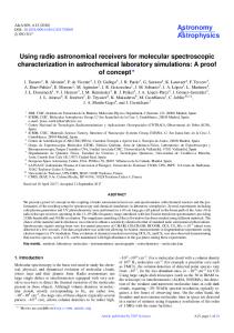
Symbol SNR (dB)
Fig. 9 – Theoretical vs. Measured results for DEMPSK reception. Graph is of BER versus ES/N0.
BPSK, QPSK, 8-PSK, 16-PSK, DBPSK, DQPSK, D-8PSK, D-16PSK, 16-QAM, 64-QAM, and 256-QAM (where the QAM constellations are rectangular).
11.1. PERFORMANCE MEASUREMENTS In Fig. 9 we see measured results from the hardware receiver for M-PSK reception. SNR was measured using both the SNR estimator of (8) and (11), which agreed to within ±0.2 dB (in Fig. 9 the estimate of (8) was used). The coding of the symbols is differential (to resolve the inherent M-fold carrier ambiguity), and the symbol mapping is gray coded (in order to reduce the probability of multiple-bit errors when a symbol error occurs [24, 26]). The demodulation is coherent, and so this type of communications link is called DEMPSK (Differentially Encoded M-PSK [24 Chap. 4]). For comparison, in Fig. 9 theoretical predictions are shown. For DEBPSK, the theoretical bit-error rate in Fig. 9 is given as [24 eq. 4.12] erfc 1 0.5 erfc . For M 2 , while
exact bit-error rate formulas for gray-coded DEMPSK can be derived [24 Chap. 4, 26 Sec. 5.2.7], it can be shown that a simple and sufficiently accurate approximate bit-error rate formula for this type of link is [24 Chap. 4, 26 Sec. 5.2.7]:
Pb
erfc lo g 2 M 2
M
sin
(36)
and the theoretical predictions of (36) are those plotted for M 2 in Fig. 9. As seen in Fig. 9, the measured results are in excellent agreement with the theoretical predictions. This proves that the structures discussed in this paper have excellent performance and are suitable for practical usage.
11.2. LOOKUP TABLE SIZES In the implementation, all of the lookup tables were implemented inside the Spartan 3A FPGA, using internal BlockRam memories. The structures worked well using that setup, but to improve performance even more some lookup tables were moved to external FLASH memories, where more address bits were available, hence reducing quantization effects. To reduce memory requirements even more, and due to the fact that the symbol rate was low and
hence allowed this optimization, TDM access to the lookup tables was done, as detailed in Sec. 6.5. It should be noted that the Spartan 3A FPGA used is relatively inexpensive (<$15) and more potent FPGAs, such as the newer Xilinx Virtex series FPGAs, have more than sufficient internal memories to accommodate all of the lookup tables used. Here we present some example results for lookup table sizes that were used in the current hardware implementation. Obviously, the size for other implementations will vary as a function of the allowable quantization noise effects and available logic. 11.2.1. PHASE DETECTOR, LOCK DETECTOR, AND TED The lookup tables which correspond to LUT III and LUT VI were implemented as a single LUT lookup table accessed in a TDM fashion. The LUT size was 64 KBytes (16 address bits, 8 bit output) in FLASH memory. LUT VII was implemented as a 64 KBytes (16 address bits, 8 bit output) lookup table in FLASH memory. The four lookup tables needed for the TED of (25)-(27) (two of which are shown in Fig. 5 for the I-channel) were implemented as a single 64 Kbyte LUT in FLASH memory (16 address bits, 8 bit output) accesses in a TDM fashion. It should be noted that during the development process all the above LUTs were implemented in internal BlockRam memories as 4096-bit tables (9 address bits, 8 output bits) and this resulted in very good performance. Implementation in FLASH memory freed up internal FPGA resources while reducing quantization noise effects. 11.2.2. SNR ESTIMATION The modified structure of Sec. 6.2 was used to allow for LUT IV and LUT VIII to be implemented using a 4096bit BlockRam memory each (256 locations x 16 output bits = 4096 bits). This provided SNR estimates in dB up to a precision of 0.01 dB. For the estimator of (11), LUT I and LUT II were implemented as one single LUT that
Fig. 10 – Time-lapse graph of BPSK demodulated signal after matched filters. Top: I channel. Bottom: Q channel.
Fig. 11 – Time-lapse X-Y graph of QPSK demodulated I and Q signals after matched filters and downsampling to 10 samples/symbol. Symbol transition paths are evident.
implemented x / x 2 y 2 and which was accessed in a TDM fashion four times with the different appropriate operands for x and y (see Fig. 3), hence computing all four operations contained in LUT I and LUT II. The LUT size was 64 KBytes (16 bits address, 8 bit output).
11.3. MISCELLANEOUS MEASUREMENTS To conclude this section, we present various measured oscilloscope screenshots obtained from the hardware communications link. Apart from their graphical beauty, these screenshots give photographic evidence of the applicability and capabilities of the proposed structures. In Fig. 10 we see a demodulated BPSK signal I and Q arms. As expected, the Q channel contains no energy while the demodulated bits are in the I channel. The time-lapse nature of the picture allows us to see the eye-diagram of the signal, which confirms the good performance of the receiver.
Fig. 12 – Time-lapse X-Y graph of 8-PSK demodulated I and Q signals after the matched filters in the receiver. Symbol transition paths are evident.
In Fig. 11 we see an X-Y graph of the I and Q channels of the post-matched-filter QPSK signal, after downsampling to 10 samples/symbol. In Fig. 12 we see a similar graph for 8-
PSK, but before the downsampling operation. In both figures, the symbol transitions can clearly be seen. In Fig. 13 - Fig. 15 we see demodulated QAM-16, QAM64, and QAM-256 constellations, respectively. The demodulation of these signals was done using the structures for QPSK, as explained in Sec. 9. Clearly, as these figures show, the proposed structures are useful for QAM demodulation.
12. CONCLUSIONS We have presented a new architecture for coherent M-PSK receivers, the Linn Architecture. This architecture covers the structures of carrier PLL phase detection, carrier PLL lock detection, symbol timing error detection, symbol timing PLL lock detection, SNR estimation, PLL architecture design, loop filter design, and built-in self test. Performance results for M-PSK modulations obtained from a hardware receiver were presented, and show that the proposed architecture is viable and has excellent performance. Applications to related modulations, including QAM, CPM, offset modulations, hierarchical modulations and cognitive radio were also briefly outlined. The proposed architecture is distinguished by the fact that it is compact to implement in fixed-point hardware, is resilient to imperfections in the AGC circuit, and has excellent performance. Inherent in this architecture is a constant striving towards efficiency in digital logic resource usage and low power consumption. For all of the above reasons, the proposed architecture is very suitable for implementation of hybrid and all-digital receivers for contemporary wireless communications systems, especially those based upon FPGAs or ASICs.
Fig. 13 – QAM-16 demodulated signal constellation.
Fig. 14 – QAM-64 demodulated signal constellation.
REFERENCES [1] J. P. Costas, "Synchronous communications (classic paper republication)," Proc. of the IEEE, vol. 90, no. 8, pp. 14611466, Aug. 2002. [2] D. P. Taylor, "Introduction to 'Synchronous Communications'," Proc. of the IEEE, vol. 90, no. 8, pp. 1459-1460, Aug. 2002. [3] P. B. Kenington, RF and baseband techniques for software defined radio. Boston: Artech House, 2005. [4] H. Meyr, M. Moeneclaey, and S. Fechtel, Digital communication receivers: synchronization, channel estimation, and signal processing. NY: Wiley, 1998. [5] U. Mengali and A. N. D'Andrea, Synchronization techniques for digital receivers. NY: Plenum Press, 1997. [6] Y. Linn, "Robust M-PSK phase detectors for carrier synchronization PLLs in coherent receivers: theory and simulations," IEEE Trans. Commun., vol. 57, no. 6, pp. 17941805, Jun. 2009. [7] Y. Linn, "An Optimal Adaptive M-PSK Carrier Phase Detector Suitable for Fixed-Point Hardware Implementation within FPGAs and ASICs," in Proc. IEEE 2006 Workshop on Signal Processing Systems (SiPS'06), Banff, AB, Canada, Oct. 2-4, 2006, pp. 238-243. [8] Y. Linn, "A Robust Phase Detection Structure for M-PSK: Theoretical Derivations, Simulation Results, and System Identification Analysis," in Proc. 18th Canadian Conference on Electrical and Computer Engineering (CCECE’05), Saskatoon, SK, Canada, May 1-4, 2005, pp. 869-883.
Fig. 15 – QAM-256 demodulated signal constellation. [9] Y. Linn, "Synchronization, Phase Detection, Lock Detection, and SNR Estimation in Coherent M-PSK Receivers," Ph.D. thesis, Electrical and Computer Engineering, University of British Columbia, July 2007. [10] Y. Linn, Synchronization in Coherent M-PSK Receivers: Carrier Synchronization, Phase Detection, Lock Detection, and SNR Estimation. Saarbruecken, Germany: VDM Verlag, 2008. [11] Y. Linn and N. Peleg, "A family of self-normalizing carrier lock detectors and Es/N0 estimators for M-PSK and other
[12]
[13]
[14]
[15] [16]
[17]
[18]
[19]
[20]
[21]
[22]
[23]
[24] [25] [26]
phase modulation schemes," IEEE Trans. Wireless Commun., vol. 3, no. 5, pp. 1659-1668, Sep. 2004. Y. Linn, "Simple and Exact Closed-Form Expressions for the Expectation of the Linn-Peleg M-PSK Lock Detector," in Proc. 2007 IEEE Pacific Rim Conference on Communications, Computers and Signal Processing (PACRIM'07), Victoria, BC, Canada, Aug. 22-24, 2007. Y. Linn, "A new NDA timing error detector for BPSK and QPSK with an efficient hardware implementation for ASICbased and FPGA-based wireless receivers," in Proc. 2004 IEEE Intl. Symp. on Circuits and Systems (ISCAS'04), Vancouver, BC, Canada, May 23-26, 2004, pp. IV:465-468. Y. Linn, "Two new decision directed M-PSK timing error detectors," in Proc. 18th Canadian Conference on Electrical and Computer Engineering (CCECE’05), Saskatoon, SK, Canada, May 1-4, 2005, pp. 1759-1766. Y. Linn, "A self-normalizing symbol synchronization lock detector for QPSK and BPSK," IEEE Trans. Wireless Commun., vol. 5, no. 2, pp. 347-353, Feb. 2006. Y. Linn, "A symbol synchronization lock detector and SNR estimator for QPSK, with application to BPSK," in Proc. 3rd IASTED International Conference on Wireless and Optical Communications (IASTED WOC'03), Banff, AB, Canada, Jul. 14-16, 2003, pp. 506-514. Y. Linn, "A Carrier-Independent Non-Data-Aided Real-Time SNR Estimator for M-PSK and D-MPSK Suitable for FPGAs and ASICs," IEEE Trans. Circuits and Systems I, vol. 56, no. 7, pp. 1525-1538, Jul. 2009. Y. Linn, "Quantitative analysis of a new method for real-time generation of SNR estimates for digital phase modulation signals," IEEE Trans. Wireless Commun., vol. 3, no. 6, pp. 1984-1988, Nov. 2004. Y. Linn, "A Hardware Method for Real-Time SNR Estimation for M-PSK using a Symbol Synchronization Lock Metric," in Proc. 9th Canadian Workshop on Information Theory, Montréal, QC, Canada, Jun. 5-8, 2005, pp. 247-251. Y. Linn, "A Real-Time SNR Estimator for D-MPSK over Frequency-Flat Slow Fading AWGN Channels," in Proc. 2006 IEEE Sarnoff Symposium, Princeton, NJ, Mar. 27-28, 2006. Y. Linn, "A Methodical Approach to Hybrid PLL Design for High-Speed Wireless Communications," in Proc. 8th IEEE Wireless and Microwave Technology Conf. (WAMICON 2006), Clearwater, FL, Dec. 4-5, 2006. Y. Linn, "Efficient Loop Filter Design in FPGAs for Phase Lock Loops in High-Datarate Wireless Receivers – Theory and Case Study," in Proc. 6th Annual Wireless Telecommunications Symposium (WTS 2007), Pomona, CA, Apr. 26-28, 2007. Y. Linn, "Efficient Structures for PLL’s Loop Filter Design in FPGAs in High-Datarate Wireless Receivers – Theory and Case Study," in Wireless technology: applications, management, and security, S. Powell and J. P. Shim, Eds., 1st ed. New York: Springer, 2009. F. Xiong, Digital modulation techniques. Boston: Artech House, 2000. F. M. Gardner, "Interpolation in digital modems. I. Fundamentals," IEEE Trans. Commun., vol. 41, no. 3, pp. 501-507, Mar. 1993. J. G. Proakis, Digital communications, 4th ed. Boston: McGraw-Hill, 2001.
[27] M. R. Spiegel, Mathematical handbook of formulas and tables. NY: McGraw-Hill, 1968. [28] F. M. Gardner, "A BPSK/QPSK timing-error detector for sampled receivers," IEEE Trans. Commun., vol. 34, no. 5, pp. 423-429, May 1986. [29] K. H. Mueller and M. Muller, "Timing recovery in digital synchronous data receivers," IEEE Trans. Commun., vol. 24, no. 5, pp. 516-530, May 1976. [30] W. C. Lindsey and M. K. Simon, Telecommunication systems engineering. NJ: Prentice-Hall, 1973. [31] Y. Linn, "A Tutorial on Hybrid PLL Design for Synchronization in Wireless Receivers," in Proc. International Seminar: 15 Years of Electronic Engineering, Universidad Pontificia Bolivariana, Bucaramanga, Colombia, Aug. 15-19, 2006 (invited paper). [32] Y. Linn, "Synchronization and Receiver Structures in Digital Wireless Communications (workshop notes)," in International Seminar: 15 Years of Electronic Engineering. Universidad Pontificia Bolivariana, Bucaramanga, Colombia, Aug. 15-19, 2006. [33] M. Seimetz, High-order modulation for optical fiber transmission, 1st ed. New York: Springer, 2009. [34] M. Simon and J. Smith, "Carrier Synchronization and Detection of QASK Signal Sets," IEEE Trans. Commun., vol. 22, no. 2, pp. 98-106, Feb. 1974. [35] Y. Linn, "An Ultra Low Cost Software Defined Radio Laboratory for Education and Research," in Proc. Intl. Conf. Software Defined Radio 2009 (SDR'09), Washington DC, Dec. 1-4, 2009. [36] Y. Linn, "Bridging the Wireless Communications Education Digital Divide: a Low-Cost Laboratory for Wireless Communications Teaching and Research," in Proc. Latin America Workshop on Communications, Medellín, Colombia, Sep. 8-11, 2009. [37] M. J. Yedlin and Y. Linn, "A Novel Method for Travel-Time Measurement for Geophysical Inversion Problems," in Proc. 2006 IEEE International Geoscience and Remote Sensing Symposium (IGARSS'06), Denver, CO, Jul. 31 - Aug. 4, 2006, pp. 1523-1526. [38] Y. Linn and M. J. Yedlin, "A Simulator for Differential MSK Direct Sequence Spread Spectrum Systems Operating in a Multipath AWGN Environment, with Applications to Acoustic Travel-Time Measurement," in Proc. 8th ACM/IEEE International Symposium on Modeling, Analysis and Simulation of Wireless and Mobile Systems (MSWIM 2005), Montréal, Québec, Canada, Oct. 10-13, 2005, pp. 47-58 (in Poster Paper Proceedings). [39] W. Fischer, Digital video and audio broadcasting technology: a practical engineering guide, 2nd ed. New York: Springer, 2008. [40] S. O'Leary, Understanding digital terrestrial broadcasting. Boston, MA: Artech House, 2000. [41] J. Hamkins and M. K. Simon, Autonomous software-defined radio receivers for deep space applications. Hoboken, N.J.: Wiley-Interscience, 2006. [42] Y. Linn, "Generation of Bandpass Gaussian Noise with Applications to Complete Built In Self Test in Wireless Communications Receivers," in Proc. IEEE ComSoc LATINCOM, Medellín, Colombia, Sept. 10-11, 2009.